

80
.pdfКупчишин А.И. и др.
11 А.I. Kupchishin, B.G. Taipova, V.M. Lisitsyn, A.A. Kupchishin, N.A. Voronova and V.I. Kirdiashkin, 12th Intern. Conf. on Gas Discharge Plasmas and Their Applications (Journal of Physics, 2015), р. 1-4.
12 A.P. Surzhikov, O.V. Galtseva, E.A. Vasendina, V.A. Vlasov and E.V. Nikolaev, Materials Science and Engineering, 110 012002, 1-4 (2016).
13 V.E.Wildeman, Experimental studies of the properties of materials under complex thermomechanical effects (M.: Fizmatlit, 2012), 203 с. (in Russ).
14 A.I. Kupchishin, B.G. Taipova, A.A. Kupchishin, N.A. Voronova, V.I. Kirdyashkin and T.V. Fursa, Material Science and Engineering 110 012037, 1-5 (2016) doi: 10.1088/1757-899X/110/1/012037.
15 A.I. Kupchishin, A.A. Kupchishin, N.A. Voronova, V.I. Kirdyashkin, and V.A. Gyngazov, Material Science and Engineering 110 012039, 1-4 (2016) doi: 10.1088/1757-899X/110/1/012039.
16 V.V. Zuev, M.V. Uspenskaya and A.O. Olekhnovich Physics and chemistry of polymers: Studies. Allowance (St. Petersburg.: SPbSU ITMO, 2010), 45 p. (in Russ).
17M.H. Mukhametrakhimov, Fundamental problems of modern materials science, 10, 1, 82-86 (2013).
18Yu.K. Mashkov, Z.N. Ovchar, V.I. Surikov, and L.F. Kalistratova, Composite materials based on polytetrafluoroethylene (Moscow: Mashinostroenie, 2005), 239 с. (in Russ).
19Surface Engineering for Enhanced Performance against Wear/ by ed. M. Roy. (Springer-Verlag Wien., 2013), 319 p.
20T.N. Koltunowich, P. Zhukowski, V. Bondariev, J.A. Fedotiva, and A.K. Fedotov, Acta Physica Polonica A, 123, 5, 932934 (2013).
ISSN 1563-0315 |
Recent Contributions to Physics. №3 (66). 2018 |
61 |
IRSTI 47.09.48
Kenzhina I.E.1,2*, Kozlovskiy A.L.1,2, Petrov A.V.3, Kadyrzhanov K.K.1
1The Institute of Nuclear Physics of Republic of Kazakhstan, Kazakhstan, Astana
2L.N. Gumilyov Eurasian National University, Kazakhstan, Astana
3SSPA "Scientific-Practical Materials Research Centre of NAS of Belarus, Belarus, Minsk, *e-mail: kenzhina@physics.kz
SYNTHESIS OF CU/CUO NANOSTRUCTURES
Among the variety of synthesized nanostructures, a special place is occupied by Cu nanotubes, due to their physical-chemical and electrical properties, and also because of potential applications in microelectronics. In this paper, we present the results of studies of copper nanostructures synthesis in the form of hollow nanotubes obtained by electrochemical deposition in pores of template matrices based on polymer matrices at polyethylene terephthalate. Electrochemical synthesis in tracks of the template was carried out in potentiostatic mode at a voltage of 0.5 to 1.5 V. By controlling the deposition time, the difference in the applied potentials, the electrolyte temperature, we can change the geometric parameters of synthesized nanostructures. The electrolyte temperature was 25 - 50 °C. Morphology, crystal structure, element and phase composition of nanostructures were studied using the methods of scanning electron microscopy, energy dispersive and X-ray phase analysis. Dependences of the change in structural and conductive properties of synthesized nanostructures from the synthesis conditions are established. Optimal conditions for the synthesis of Cu/CuO nanostructures of various geometries (nanowires and nanotubes) that have potential applications in microelectronics are determined.
Key words: nanostructures, nanotubes, template synthesis, conductive properties, crystal structure.
Кенжина И.Е.1,2*, Козловский A.Л.1,2, Петров А.В.3, Кадыржанов К.К.2
1Астанинский филиал Института ядерной физики, Казахстан, г. Астана 2Евразийский национальный университет им. Л.Н. Гумилева, Казахстан, г. Астана 3НПЦ НАН Беларуси по материаловедению, Беларусь, г. Минск,
*e-mail: kenzhina@physics.kz
Синтез Cu/CuO наноструктур
Среди разнообразия синтезированных наноструктур особое место занимают нанотрубки Cu из-за их физико-химических и электрических свойств, а также из-за потенциальных применений в микроэлектронике. В настоящей работе представлены результаты исследований синтеза медных наноструктур в виде полых нанотрубок, полученных электрохимическим осаждением в порах темплатных матриц на основе полимерных пленок из полиэтилентерефталата. Электрохимический синтез в треки темплатов проводился в потенциостатическом режиме при напряжении от 0,5 до 1,5 В. Контролируя время осаждения, разницу приложенных потенциалов, температуру электролита, мы можем изменить геометрические параметры синтезированных наноструктур. Морфология, кристаллическая структура, элементный и фазовый состав наноструктур были изучены с использованием методов сканирующей электронной микроскопии, энергодисперсионного и рентгенофазового анализа. Установлены зависимости изменения структурных и проводящих свойств синтезированных наноструктур от условий синтеза. Определены оптимальные условия для синтеза Cu/CuO наноструктур различной геометрии (нанопроволоки и нанотрубки), которые имеют потенциальные применения в микроэлектронике.
Ключевые слова: наноструктуры, нанотрубки, матричный синтез, электропроводящие свойства, кристаллическая структура.
© 2018 Al-Farabi Kazakh National University

Kenzhina I.E. et al.
Кенжина И.Е.1,2*, Козловский A.Л.1,2, Петров А.В.3, Қадыржанов Қ.К.2
1Ядролық физика Институтының филиалы, Қазақстан, Астана қ.
2Гумилев атындағы Еуразия ұлттық университеті, Қазақстан, Астана қ.
3Белоруссияның Ұлттық ғылым академиясының материалтану бойынша Ғылыми-Практикалық Орталығы, Беларусь, Минск қ.,
*e-mail: kenzhina@physics.kz
Cu/CuO наноқұрылымдардың синтезі
Синтезделген наноқұрылымдардың алуан түрлерінің арасында физика-химиялық және электр қасиеттеріне, сондай-ақ микроэлектроникадағы әлеуетті қосымшаларға байланысты Cu нанотүтікшелері ерекше орын алады. Осы мақалада біз полиэтилентерефталат жасалған полимерлік пленкалар негізінде матрицаларды үлгілеуде электрохимиялық тұндыру арқылы алынған қуыстық нанотүтікшелер түріндегі мыс наноқұрылымдарының синтезін зерттеу нәтижелерін ұсынамыз. Темплаттардың тректеріндегі электрохимиялық синтез потенциостатикалық режимде 0,5 - 1,5 В кернеуде жүргізілді. Тұндыру уақытын, қолданылатын потенциалдардағы айырмашылықты, электролиттің температурасын бақылау арқылы синтезделген наноқұрылымдардың геометриялық параметрлерін өзгерте аламыз. Наноқұрылымдардың морфологиясы, кристалды құрылымы, элементі және фазалық құрамы сканерден өтетін электронды микроскопия, энергодисперсті және рентгендік фазалық талдау арқылы зерттелген. Синтезделген наноқұрылымдардың құрылымдық және өткізгіш қасиеттеріндегі синтез жағдайында өзгерістердің тәуелділігі анықталды. Микроэлектроникадағы әлеуетті қосымшалары бар әртүрлі геометрияның (наносымдар және нанотүтікшелер) Cu/CuO наноқұрылымдарын синтездеудің оңтайлы шарттары анықталды.
Түйінді сөздер: наноқұрылымдар, нанотүтікшелер, матрицалық синтез, электр өткізгіш қасиеттері, кристалды құрылым.
Introduction |
Experimental |
Among the variety of synthesized nanostructures, a special place is occupied by Cu nanotubes, due to their physical-chemical and electrical properties, and also because of potential applications in microelectronics [1-5]. The method of electrochemical deposition for synthesizing nanostructures is distinguished. That makes it possible to control the morphology and structural properties of synthesized nanostructures. The use of porous matrices possesses high thermal and chemical stability enable to easily control the geometry of deposited nanostructures over large areas. Varying the synthesis conditions such as the electrolyte temperature or the potential difference leads to a change in the structural and conductive properties of nanostructures, this directly affects their potential application in the future [6-11].
In this paper, we present the results of studies of copper nanostructures synthesis in the form of hollow nanotubes obtained by electrochemical deposition in pores of template matrices based on polymer matrices at polyethylene terephthalate. Dependences of the influence of the difference between the deposition potentials and the temperature of the electrolyte solution on structural and conductive properties, the elemental composition, and the degree of crystallinity are presented.
Track membranes were obtained of polyethylene terephthalate of «Hostaphan®» brand manufactured by Mitsubishi Polyester Film (Germany). The films were irradiated at DC-60 accelerator of heavy ions (Kazakhstan) with accelerated krypton ions with an energy of 1.75 MeV/nucleon and a fluence of 4×10⁷ ion/cm2. The membranes were etched according to the standard double-sided etching technique in a solution of 2.2 M NaOH at 85 ± 1 °C. The pore size according to gas porosimetry, and SEM was 380 ± 10 nm, the track length was 12 μm.
Electrochemical synthesis in tracks of the template was carried out in potentiostatic mode at a voltage of 0.5 to 1.5 V. The electrolyte temperature was 25 - 50 °C. The composition of the electrolyte solution: CuSO4·5H2O (238g/l), H2SO4 (21g/l). The yield of copper by current from the sulfuric acid solutions of electrolytes is 100%. The growth of nanostructures was monitored by the chronoamperometry method with the "Agilent 34410A" multimeter. Since the template PET matrices are dielectric, a layer of gold with a thickness of no more than 10 nm, which is further a working electrode (cathode) during electrochemical deposition, was deposited to create a conductive layer by magnetron sputtering in a vacuum. By controlling the deposition time, the difference in
ISSN 1563-0315 |
Recent Contributions to Physics. №3 (66). 2018 |
63 |

Synthesis of Cu/CuO nanostructures
the applied potentials, the electrolyte temperature, we can change the geometric parameters of synthesized nanostructures. All possible reactions associated with the synthesis process are listed
below.
CuSO4 → Cu+2 + SO4-2
Cu+2 + 2e → Cu(s) ↓
Copper sulfate dissociates into Cu+2 and SO4-2 ions in the first stage of electrolysis. Then Cu+2 ions are reduced near the cathode to Cu(s), and a layer is formed behind the wall layer of the nanostructures in pores, repeating the template geometry. Because of the change in concentration of H+ ions during the synthesis, the pH of the solution can vary, which leads to uneven filling of the pores. To control pH of the solution, sulfuric acid H2SO4 was used, acting as a buffer to maintain the pH.
Investigation of structural characteristics and elemental composition of nanostructures obtained before and after irradiation was carried out using a scanning electron microscope "Hitachi TM3030" with a microanalysis system "Bruker XFlash MIN SVE" at an accelerating voltage of 15 kV. X-ray diffraction analysis (XRD) was performed on a D8 ADVANCE ECO diffractometer (Bruker, Germany) using CuKα radiation. The software BrukerAXSDIFFRAC.EVAv.4.2 and the international ICDD PDF-2 database were used to identify the phases and study the crystal structure.
Results and Discussion
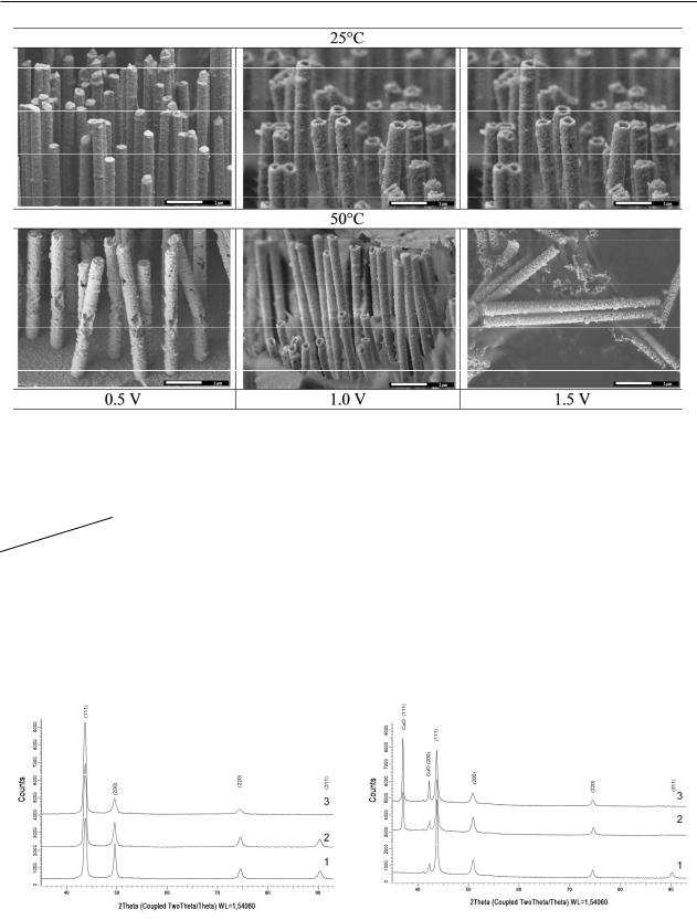
Figure 1 shows SEM images of synthesized nanostructures under different synthesis conditions.
Analysis of electronic images of synthesized samples showed that the synthesized nanostructures are hollow nanotubes whose height coincides with the thickness of the template matrix of 12 μm. The diameter of nanotubes corresponds to pore diameters of 380 ± 10 nm. It is seen that at a potential difference of 0.5 V, formation of continuous nanostructures in the form of nanowires is observed according to SEM images. In this case,
an increase in the temperature of the electrolyte leads to the formation of cavities and loose areas in nanostructures. This can be caused by a nonuniform deposition process. At potential differences of 1.0 and 1.5 V, the formation of hollow nanostructures in the form of nanotubes is observed. While an increase in the temperature of the electrolyte leads to a decrease in the wall thickness and growth height heterogeneity at an electrolyte temperature of 50 ° C for a potential difference of 1.0 V. For a potential difference of 1.5 V, increase of electrolyte temperature leads to the formation of loose hollow nanotubes consisting of large nanoparticles. As can be seen from SEM images presented, an important is the difference in the process of forming the wall thickness is the applied potential difference and the electrolyte temperature. They directly depend on the rate of formation of metal ions and the rate of their diffusion in solution. The change in the difference between the applied potentials and electrolyte temperature affects the growth rate of nanostructures. A decrease in the wall thickness is observed during the growth process for large potential differences and electrolyte temperatures. This may be due to the rapid formation of nuclei of crystallites, from which nanostructures are formed. However, this process is accompanied by negative factors. With increasing current density due to the increase in the potential difference at electrodes during the growth of nanostructures, adsorption of hydrogen impurities, anions of salts, and also hydroxides is observed. Some of them deposited on the surface of template matrix, but some of the precipitate formed is included in the crystal structure of nanostructures growing in pores.
X-ray phase and energy dispersive analysis methods were used to assess the effect of deposition conditions on the elemental composition and crystal structure. Table 1 presents the data of the elemental composition of synthesized samples. The reliability of the results was confirmed by taking spectra from five points along the surface of investigated sample, as well as obtaining the distribution maps of elements in the structure using the mapping method.
64 |
Хабаршы. Физика сериясы. №3 (66). 2018 |
Kenzhina I.E. et al.
Figure 1 – SEM images of synthesized nanostructures under different synthesis conditions
Table 1 – Elemental analysis of synthesized samples
U,V |
T,°C |
25 |
50 |
|
|||
|
|
|
|
0.5 |
|
|
Cu92O8 |
1.0 |
|
Cu100 |
Cu74O26 |
1.5 |
|
|
Cu62O38 |
As can be seen from the presented results at an electrolyte temperature of 25 °C, the synthesized
nanostructures are single-component structures consisting of copper without impurities of oxide compounds. An increase in the temperature of the electrolyte to 50 °C leads to the formation of copper structures with oxide impurities in the structure. The presence of oxide compounds in the structure of nanotubes can be due to the rapid release of oxygen and hydrogen during the synthesis, while the oxide compounds can lead to partial amorphization of nanostructures.
25°C |
50°C |
Figure 2 – XRD diffractograms of investigated samples of Cu nanostructures: 1) 0.5 V; 2) 1.0 V; 3) 1.5 V
ISSN 1563-0315 |
Recent Contributions to Physics. №3 (66). 2018 |
65 |

Synthesis of Cu/CuO nanostructures
Figure 2 shows X-ray diffraction patterns of investigated samples. The diffraction patterns of investigated samples are characteristic for X-ray diffraction on polycrystalline nanoscale structures (broadened low-intensity peaks). The deviation of peaks of investigated samples from the symmetrical shape is observed with a change in the synthesis conditions, which indicates the presence in the structure of microarrays and deformation arising during the synthesis. Analysis of samples diffractograms made it possible to establish that the Cu nanostructures studied possess a polycrystalline structure with a fcc phase.
The unit cell parameters for investigated samples were determined in processing the obtained X-ray diffractograms. The crystal lattice parameter was calculated using the Nelson-Taylor extrapolation function (4) [27]:
|
|
|
2 |
2 |
|
|
|
а f |
1 |
cos |
cos |
|
, |
(4) |
|
|
2 |
|
sin |
|
|
|
|
|
|
|
|
|
|
|
|
|
|
|
|
|
|
|
|
The value and error in determining a parameter are obtained by linear extrapolation of this function to the zero value of the argument (θ = 90 °). The average size of crystallites was determined by the Scherer equation. The results of the change in the main characteristics of the crystal structure for investigated samples are shown in Table 2.
Table 2 – Data on changes in characteristics of the crystal structure
U,V |
|
a,Å |
Crystallinity, |
L, nm |
||
|
|
|
% |
|||
|
|
|
|
|
|
|
T,°С |
|
|
|
|
|
|
25 |
50 |
25 |
50 |
25 |
50 |
|
|
|
|
|
|
|
|
0.5 |
3.6052 |
3.6178 |
89 |
78 |
15.7 |
25.6 |
1.0 |
3.6131 |
3.6215 |
84 |
67 |
18.3 |
29.4 |
|
|
|
|
|
|
|
1.5 |
3.6141 |
3.6314 |
81 |
54 |
19.6 |
41.5 |
|
|
|
|
|
|
|
The change in FWHM of the main diffraction line (111) on X-ray diffraction patterns indicates a change in the degree of crystallinity of synthesized samples. When the lines on the diffractogram were approximated by the necessary number of symmetric pseudo-Voigt functions, the width of the registered FWHM lines was determined. It made it possible to characterize the perfection of the crystal structure and to assess the degree of crystallinity.
The results of evaluation are presented in Table 2. As can be seen from the presented data, samples obtained at room temperature have the highest degree of crystallinity. When nanowires are formed, the crystallinity is the highest and is 89%. In turn, at a temperature of 50 °C and an increase in the potential difference from 1.0 to 1.5 V, a sharp decrease in the degree of crystallinity is observed, which is due to amorphous inclusions in the structure. In this case, the change in the intensity and shape of diffraction peaks can be caused by the imperfection of the crystal structure, as well as to the defects formed during the synthesis of nanotubes. The presence of first-order defects (point defects, dislocation loops, particles of a new phase) in the structure leads to a shift in the diffraction maxima, but they do not affect the broadening of the diffraction lines. Defects of the second kind (dislocations, accumulation of defects) cause broadening of the diffraction lines.
The change in the intensities of diffraction peaks can be due to the change in the texture planes and the reorientation of crystallites. The texture coefficients were calculated according to the Harris formula (1) [12]:
TC(hkl) |
I(hkl) |
1 |
|
I(hkl) |
, (1) |
I0 (hkl) |
n |
I0 (hkl) |
where I(hkl) is the experimentally obtained relative intensity; I0(hkl) is the relative intensity corresponding to a given plane according to the JCPDS base; n is the number of planes. The results are shown in Table 3. The texture coefficients greater than one point to the predominant orientation of the array of nanotubes along the corresponding directions, which implies an increase in the number of grains along these directions. The number of reflections (n) corresponds to the maximum value of texture coefficients.
As can be seen from the presented data, a change in the deposition conditions results in a change in the texture coefficients and a reorientation of texture planes in nanostructures. In this case, an increase in the potential difference at an electrolyte temperature of 25 °C leads to the appearance of a distinguished texture direction in (111) plane. While at a temperature of 50 °C, an increase in the potential difference leads to a decrease in the texture coefficients and the absence of a specified texture direction.
66 |
Хабаршы. Физика сериясы. №3 (66). 2018 |

Kenzhina I.E. et al.
Table 3 |
– Results of calculations of texture coefficients |
|
|
|
|
|
|
|
|
|
|
|
|
|
|
|
|
|
|
hkl |
|
|
TC(hkl) |
|
|
|
|
T,°C |
U,V |
|
25 |
|
|
50 |
|
|
|
|
|
|
|
|
|
|
|
|
|
0.5 |
1.0 |
1.5 |
0.5 |
1.0 |
1.5 |
|
|
111 |
1.1351 |
1.6411 |
1.8965 |
1.6737 |
1.3622 |
0.9853 |
|
|
200 |
1.1211 |
1.0872 |
0.5517 |
0.8636 |
0.7639 |
0.5311 |
|
|
220 |
0.5414 |
0.4673 |
0.3131 |
0.4316 |
0.2415 |
0.1135 |
|
|
311 |
0.4341 |
0.3461 |
- |
0.2351 |
- |
- |
Conclusion
As a result of the study, Cu/CuO nanostructures with a diameter of 380 nm were synthesized using the electrochemical synthesis method. The influence of the potential difference and the electrolyte temperature on the change in structural and conductive
properties, phase and elemental composition was studied. Dependences of the change in structural and conductive properties of synthesized nanostructures on the synthesis conditions are established. Optimal conditions for the synthesis of Cu/CuO nanostructures of various geometries (nanowires and nanotubes) that have potential applications in microelectronics are determined.
References
1Gutiérrez-Hernández J. M. et al. In vitro evaluation of osteoblastic cells on bacterial cellulose modified with multi-walled carbon nanotubes as scaffold for bone regeneration // Materials Science and Engineering: C. – 2017. – Vol. 75. – P. 445-453.
2Ahmad N. et al. AC Potential-Dependent Concentration Variation and Domain Wall Pinning in Co 1− x Zn x (x= 0.4− 0.5) Nanorods // Journal of Superconductivity and Novel Magnetism. – 2016. – Vol. 29. – №. 2. – P. 509-513.
3Wen X., Long M., Tang A. Flake-like Cu2O on TiO2 nanotubes array as an efficient nonenzymatic H2O2 biosensor // Journal of Electroanalytical Chemistry. – 2017. – Vol. 785. – P. 33-39.
4Yan Y. et al. Processing, characterisation and electromechanical behaviour of elastomeric multiwall carbon nanotubes-poly (glycerol sebacate) nanocomposites for piezoresistive sensors applications // Composites Science and Technology. – 2017. – Vol.
142.– P. 163-170.
5Panchakarla L. S., Reshef T. Inorganic Nanotubes and Fullerene Like Nanoparticles at the Crossroad between Materials Science and Nanotechnology and Their Applications with Regard to Sustainability // Nanotechnology for Energy Sustainability. – 2017. – P. 745-80.
6Yang H. et al. Electrochemical sensor for rutin detection based on Au nanoparticle-loaded helical carbon nanotubes // Journal of Nanoparticle Research. – 2017. – Vol. 19. – №. 10. – P. 354.
7Wu Y. et al. Localized surface plasmon resonance in graphene nanomesh with Au nanostructures // Applied Physics Letters. – 2016. – Vol. 109. – №. 4. – P. 041106.
8Kim T., Park D. Preparation and characterization of Ni nanostructures coated on the substrates for glycerol steam reforming // Journal of nanoscience and nanotechnology. – 2017. – Vol. 17. – №. 4. – P. 2478-2481.
9Bañobre-López M. et al. A colloidally stable water dispersion of Ni nanowires as an efficient T 2-MRI contrast agent // Journal of Materials Chemistry B. – 2017. – Vol. 5. – №. 18. – P. 3338-3347.
10Medina J.L.T. et al. Large magnetic anisotropy enhancement in size controlled Ni nanowires electrodeposited into nanoporous alumina templates // Nanotechnology. – 2016. – Vol. 27. – №. 14. – P. 145702.
11Seshadri I. et al. Microwave synthesis of branched silver nanowires and their use as fillers for high thermal conductivity polymer composites // Nanotechnology. – 2016. – Vol. 27. – №. 17. – P. 175601.
12Harris G.B.X. Quantitative measurement of preferred orientation in rolled uranium bars // The London, Edinburgh, and Dublin Philosophical Magazine and Journal of Science. – 1952. – Vol. 43. – №. 336. – P. 113-123.
ISSN 1563-0315 |
Recent Contributions to Physics. №3 (66). 2018 |
67 |

Synthesis of Cu/CuO nanostructures
References
1 G. Hernández, Materials Science and Engineering: C 75, 445-453 (2017). https://doi.org/10.1016/j.msec.2017.02.074 2 N. Ahmad, J. Supercond. Nov. Magn. 29, 509-13, (2016). DOI 10.1007/s10948-015-3274-4
3X. Wen, Journal of Electroanalytical Chemistry. 785, 33-9, (2017). doi: 10.1016/j.jelechem.2016.12.018
4Y. Yan, Composites Science and Technology 142, 163-70, (2017). http://dx.doi.org/10.1016/j.compscitech.2017.02.007
5L. S. Panchakarla, T, Reshef, Nanotechnology for Energy Sustainability, 745-80, (2017). DOI: 10.1021/jacs.7b01652
6H. Yang, Journal of Nanoparticle Research 19.10, 354, (2017). https://doi.org/10.1007/s11051-017-4046-9
7Y. Wu, Applied Physics Letters 109.4, 041106, (2016). doi: 10.1063/1.4959833
8T. Kim, P. Daeil, Journal of Nanoscience and Nanotechnology 17.4, 2478-2481, (2017). doi.org/10.1166/jnn.2017.13353
9M. Bañobre-López, Journal of Materials Chemistry B 5.18, 3338-2247, (2017). DOI: 10.1039/C7TB00574A.
10J. Medina, Nanotechnology 27.14, 145702, (2016). doi:10.1088/0957-4484/27/14/145702
11I. Seshadri, Nanotechnology 27.17, 175601, (2016) doi:10.1088/0957-4484/27/17/175601.
12G.B. Harris, Dublin Philosophical Magazine and Journal of Science. 43, 113, (1952). https://doi.org/10.1080/14786440108520972.
68 |
Хабаршы. Физика сериясы. №3 (66). 2018 |
МРНТИ 90.03.03
Аханова Н.Е.1,2, Дарзнек С.А.3, Желкобаев Ж.Е.3, Габдуллин М.Т.1,2, Ерланулы Е.1,2*, Батрышев Д.Г.1,2
1Национальная нанотехнологическая лаборатория открытого типа, Казахский национальный университет имени аль-Фараби, Казахстан, г. Алматы,
*e-mail: yerlanuly@physics.kz
2АО «Казахстанско-Британский технический университет», Казахстан, г. Алматы 3АО «Научно-исследовательский центр по изучению свойств поверхности и вакуума», Россия, г. Москва
РАЗРАБОТКА СИСТЕМЫ ИЗМЕРЕНИЯ В НАНОДИАПАЗОНЕ
Работа посвящена измерению линейных смещений в нанодиапазоне, анализу особенностей такого рода работ, обеспечению единства измерений и стабильности измеряемой физической величины,достоверностирезультатовиихпривязкикГосэталонам.Рассмотреныкритерии,которым должны соответствовать методы и средства прецизионных измерений в нанодиапазоне, а также методы и средства съема и представления обработки получаемой информации. Сделан анализ основных источников погрешностей. Результаты этих исследований представлены в работе [1]. Рассмотрены особенности построения измерительных комплексов, а также вопросы калибровки фазовых измерений в оптике.Рассмотрены вопросы прикладного характера: измерение реальных перемещений объектов в нанодиапазоне, определения их скорости и ускорения, а также вопросы внедрения разработанных методов в область практического применения. Приведены результаты, полученные при решении экспериментальных и прикладных задач с использованием метода и средств численного гетеродинирования. Разработанная измерительная система «интерферометрфазометр», позволяет исследовать, в реальном масштабе времени, сложные пъезокерамические структуры используемых в различных устройствах в качестве актюаторов.
Ключевые слова: лазер, линейное перемещение, нанодиапазон, интерферометр, угол фазового сдвига (УФС).
Akhanova N.E.1,2, Darznek S.A.3, Zhelkobaev J.E.3,
Gabdullin M.T.1.2, Erlanuly E.1,2*, Batryshev D.G.1,2
1National nanotechnology laboratory of open type, Al-Farabi Kazakh National University, Kazakhstan, Almaty, *e-mail: yerlanuly@physics.kz
2JSC “Kazakh-British Technical University”, Kazakhstan, Almaty
3JSC “Research Center for the Study of Surface and Vacuum Properties”, Russia, Moscow
Development of a nanoscale measurement system
The work is devoted to measuring linear displacements in the nanoscale, analyzing the features of this kind of work, ensuring the unity of measurements and stability of the measured physical quantity, the reliability of the results and their linkage to the State Standard. The criteria that must be met by methods and means of precision measurements in the nanoscale, as well as methods and means for acquiring and presenting the information obtained. The analysis of the main sources of errors is made and the results of these studies are presented in [1]. The features of the construction of measuring systems, as well as the problems of calibration of phase measurements in optics, are considered. The problems of an applied nature are considered: the measurement of real displacement of objects in the nanoscale, their speed and acceleration, as well as the introduction of the developed methods into the field of practical application.
© 2018 Al-Farabi Kazakh National University

Разработка системы измерения в нанодиапазоне
The results obtained in solving experimental and applied problems using methods and means of numerical heterodyning are presented. The developed “interferometer-phase meter” measuring system allows online investigating of complex piezoceramic structures used in various devices as actuators.
Key words: laser, linear displacement, nanoscale, interferometry, phase shift angle (PSA).
Аханова Н.Е.1,2, Дарзнек С.А.3, Желкобаев Ж.Е.3, Ғабдуллин М.Т.1,2, Ерланұлы Е.1,2*, Батрышев Д.Г.1,2
1Ашық типті нанотехнологиялар зертханасы, әл-Фараби атындағы Қазақ ұлттық университеті, Қазақстан, Алматы қ.,
*e-mail: yerlanuly@physics.kz
2«Қазақстан-Британ техникалық университеті» АҚ, Қазақстан, Алматы қ. 3«Беттік және вакуумдық қасиеттерді зерттеудің ғылыми орталығы» АҚ, Ресей, Мәскеу қ.
Наномадиапазондағы өлшеу жүйесін әзірлеу
Жұмыс нанодиапазонда сызықтық орын ауыстыруларды өлшеуге арналған, осындай жұмыстар талдауларының ерекшеліктері өлшеу тұтастығы мен өлшенетін физикалық өлшем тұрақтылығы және нәтижелер нақтылығы мен олардың Мемлекеттік эталонға байланысын қамтамасыз ету. Нанодиапазонда прецизионды өлшемдер тәсілі мен әдістеріне, сондай-ақ орым тәсілі мен әдістеріне сәйкес болуы және алынатын ақпараттың өңделуіне ұсынылу шарттары қарастырылған. Негізгі қателік көздеріне талдау жасалынды. Бұл зерттеулер нәтижелері [1] жұмыста келтірілген. Өлшеулер кешендерінің құрылу ерекшеліктері, сонымен қатар оптикадағы фазалық өлшеулерді калибрлеу сұрақтары қарастырылды. Қолданбалы сипатының сұрақтары: нанодиапазонда нақты объектілердің орын ауыстыруын өлшеу, олардың жылдамдығы мен үдеуін анықтау, сонымен қоса практикалық қолданылу аймағында құрастырылған әдістерді енгізу мәселелеріқарастырылды. Сандық гетеродинирлау құралы мен әдісін қолдану арқылы тәжірибелік және қолданбалы есептерді шешу кезінде алынған нәтижелер келтірілген. Құрастырылған «интерферометрфазометр» жүйесі уақыттың нақты масштабында актюатор есебінде әртүрлі қондырғыларда пайдаланылатынкүрделі пъезокерамикалық құрылымын зерттеуге мүмкіндік береді.
Түйін сөздер: лазер, сызықтық орын ауыстыру, нанодиапазон, интерферометр, фазалық жылжу бұрышы (ФЖБ).
Введение
Развитие наукоемких технологий немыслимо без создания высокочувствительных методов
ивысокоточных средств измерений линейных размеров и контроля прецизионных перемещений объектов в нанодиапазоне. При этом должны быть достигнуты предельно возможные степени точности и обеспечен соответствующий метрологический уровень.
Прецизионное измерение сверхмалых перемещений необходимо для проведения фундаментальных работ, связанных с созданием нового поколения взаимосвязанных эталонов в области механических и акустических величин, при исследовании квантово-размерных эффектов, высокостабильных источников когерентного излучения, калибровки актюаторов микро
инанодиапазона и контроля техногенно – опасных объектов с целью обеспечения экологического баланса окружающей среды.
Оптимальным решением этих проблем, в долговременной перспективе, может стать внедрение в практику линейных измерений методов
исредств оптической (лазерной) интерфероме-
трии-фазометрии (нанометрии), опирающихся на фундаментальные константы и эталоны физических величин [1, 2, 3].
Фазовые (интерференционные) методы в оптике используются для измерений простран- ственно-временных изменений величины разности фаз – угла фазового сдвига (УФС) в интерференционном поле между измерительным и опорным пучками, обусловленных частотной, пространственной или поляризационной дисперсией излучения в фазовом объекте [3-8].
Оптическая (лазерная) интерферометрия
– фазометрия (нанометрия), совместно с высокоразвитой техникой фазометрии радиодиапазона, дает возможность создать высокоточные измерительные системы и заложить основы для обеспечения единства линейных измерений в микрометровом и нанометровом диапазонах, а также в радио и оптическом диапазонах
Это дало возможность создать, новый класс измерительных средств и методов, отвечающих высоким метрологическим требованиям нанотехнологий и обладающих широкими возможностями для удовлетворения запросов науки и техникивобластивысокоточныхизмерений,т.е.
70 |
Вестник. Серия физическая. №3 (66). 2018 |