

Instrumentation Sensors Book
.pdfwww.globalautomation.info
C H A P T E R 3
Basic Electrical Components
3.1Introduction
Resistors, capacitors, and inductors—these are the three basic passive elements used in electrical circuits, either as individual devices or in combination. These elements are used as loads, delays, and current limiting devices. Capacitors are used as dc blocking devices, in level shifting, integrating, differentiating, filters, frequency determination, selection, and delay circuits. Inductive devices can be extended to cover analog meter movements, relays, audio to electrical conversion, electrical to audio conversion, and electromagnetic devices. They are also the basis for transformers and motors.
3.2Circuits with R, L, and C
Passive components are extensively used in ac circuits for frequency selection, noise suppression, and so forth, and are always present as parasitic components, limiting signal response and introducing unwanted delays. These components also cause phase shift between voltages and currents, which has to be taken into account when evaluating the performance of ac circuits.
3.2.1Voltage Step Input
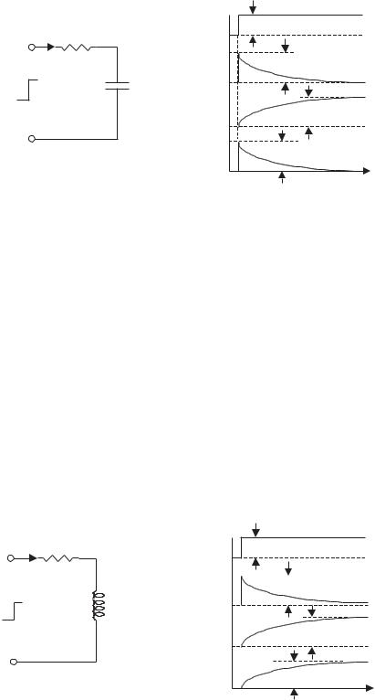
When a dc voltage is applied to the series resistor-capacitor circuit shown in Figure 3.1(a) a current flows in the elements, charging the capacitor. Figure 3.1(b) shows the input voltage step, the resulting current flowing, and the voltages across the resistor and the capacitor. Initially, all the voltage is dropped across the resistor. Although current is flowing into the capacitor, there is no voltage drop across the capacitor. As the capacitor charges, the voltage across the capacitor builds up exponentially, and the voltage across the resistor starts to decline, until eventually the capacitor is fully charged and current ceases to flow. The voltage across the capacitor is then equal to the supply voltage, and the voltage across the resistor is zero.
It should be noted that the current flowing through the resistor and into the capacitor is the same for both components, but the voltages across each component are different. That is, when the current flowing in the resistor is a maximum, the voltage across the resistor is a maximum, given by E = IR, and the voltage is said to be in phase with the current. In the case of the capacitor, the voltage is zero when the current flowing is a maximum, and the voltage is a maximum when the current is
25
www.globalautomation.info
26 |
Basic Electrical Components |
|
|
|
Input |
E |
|
I |
|
voltage |
|
|
|
|
||
|
|
|
|
|
Applied |
R |
|
Voltage |
E |
|
C |
|||
voltage |
|
across R |
||
|
|
|||
|
|
|
||
|
E |
|
Voltage |
|
|
|
|
E |
|
|
|
|
across C |
|
|
|
|
|
|
|
|
|
Current |
E/R |
|
|
|
flow |
|
|
|
|
|
|
|
|
|
|
Time |
|
(a) |
|
|
(b) |
Figure 3.1 (a) Input voltage transient to a circuit with resistance and capacitance, and (b) associated waveforms.
zero. In this case, the voltage lags the current, or there is a phase shift between the voltage and the current of 90°. The voltage across the capacitor builds up exponentially, at a rate determined by the values of the resistor and the capacitor.
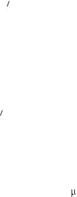
When a dc voltage is applied to a series inductance circuit resistance, as shown in Figure 3.2(a) a current will build up, Figure 3.2(b) shows the input voltage step, the resulting current buildup, and the voltages across the resistor and the inductor the inductance will initially appear as a high impedance preventing current from flowing. The current will be zero, the supply voltage will appear across the inductance, and there will be zero voltage across the resistor. After the initial turn-on, current will start to flow and build up, the voltage across the resistor will increase, and then start to decrease across the inductance. This allows the current to build up exponentially, until the current flow is limited by the resistance at its maximum value and the voltage across the inductance will be zero. The effects are similar to those that occur when a dc voltage is applied to a series R.C. network. The voltage and current in the resistor are in phase, but in the inductor are out of phase. That is,
I |
Input |
E |
|
voltage |
|||
R |
Voltage |
|
|
Applied |
E |
||
Voltage |
across L |
||
|
|||
E |
L |
|
|
|
|
||
|
Voltage |
E |
|
|
across R |
||
|
Current |
|
|
|
flow |
E/R |
|
|
|
Time |
|
(a) |
|
(b) |
Figure 3.2 (a) Input voltage transient to a circuit with resistance and inductance, and (b) associated waveforms.
3.2 Circuits with R, L, and C |
www.globalautomation.info |
27 |
in this case, the voltage appears across the inductance before the current starts to flow, and goes to zero when the current is at its maximum, so that the voltage leads the current, and there is a phase shift between the voltage and the current of 90°. The voltage across the resistor increases exponentially, at a rate determined by the value of the inductance and resistance.
3.2.2Time Constants
In an RC network when a step voltage is applied, as shown in Figure 3.1(a), the voltage across the capacitor is given by the equation [1]:
EC = E(1 − e−t RC ) |
(3.1) |
where EC is the voltage across the capacitor at any instant of time, E is the source voltage, t is the time (seconds) after the step is applied, R is in ohms and C is in farads.
Conversely, after the capacitor is fully charged, and the step input voltage is returned to zero, C discharges and the voltage across the capacitor is given by the equation:
E = Ee−t RC |
(3.2) |
C |
|
Similar equations apply to the rise and fall of currents in the inductive circuit shown in Figure 3.2(a).
Example 3.1
What is the voltage across the capacitor in Figure 3.1(a) 35 steps from 0V to 54V, if the value of the resistor is 47 kΩ  F?
F?
s after the input voltage and the capacitor is 1.5
Ec = 54(1 − e−35 × 1000000/1000 × 47 × 1000 × 1.5)V = 54 (1 − 1/e0.5)V
Ec = 54(1 − 0.606) = 21.3V
The time constant of the voltage in a capacitive circuit from (3.1) and (3.2) is defined as:
t = CR |
(3.3) |
where t is the time (seconds) it takes for the voltage to reach 63.2% of its final or aiming voltage after the application of an input voltage step (charging or discharging). For example, by the end of the first time constant, the voltage across the capacitor will reach 9.48V when a 15V step is applied. During the second time constant, the voltage across the capacitor will rise another 63.2% of the remaining voltage step; that is, (15 − 9.48)V × 63.2% = 3.49V. At the end of two time constant periods, the voltage across the capacitor will be 12.97V, and at the end of three periods, the voltage will be 14.25V, and so forth. The voltage across the capacitor reaches 99% of its aiming value in 5 CR.
28 |
www.globalautomation.info |
Basic Electrical Components |
Example 3.2
What is the time constant for the circuit shown in Figure 3.1(a), if the resistor has a value of 220 kΩ, and the capacitor is 2.2 F?
F?
t = 2.2 × 10−6 × 220 × 103 sec = 484 × 10−3 sec = 0.484 sec
The RC time constant is often used as the basis for time delays. A comparator circuit is set to detect when a voltage across a capacitor in a CR network reaches 63.2% of the input step voltage. The time delay generated is then 1 CR.
In the case of an inductive circuit, the time constant for the current is given by;
t = L R |
(3.4) |
where L is the inductance in Henrys, and t gives the time for the current to increase to 63.2% of its final current through the inductor.
Time constants apply not only to the rate of change of currents and voltages in electrical circuits when a step voltage is applied, but also to sensor outputs when there is a change in the measured variable. The output signal from the sensor changes exponentially, so that there is a delay before the sensor output reaches its final value. In the case of a temperature sensor, the time constant of the sensor is determined by factors such as its thermal mass.
3.2.3Sine Wave Inputs
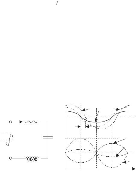
When an ac sine wave is applied to C, L, and R circuits, as shown in Figure 3.3(a) the same phase shift between voltage and current occurs as when a step voltage is applied. Figure 3.3(b) shows the relationship between the input voltage, the current flowing and the voltage across C, L, and R as can be seen. In resistive elements, the current and voltage are in phase; in capacitive circuits, the current leads the voltage
E |
I |
VR |
R |
|
|
I |
|
|
θ |
|
|
C |
|
|
AC Input E |
|
VC |
|
|
VC+ VL |
L |
|
|
|
|
VL |
90° |
180° |
270° |
|
|
Time |
(a) |
(b) |
|
Figure 3.3 (a) Series R, C, and L circuits, and (b) waveforms and phase relations in a series circuit.
3.2 Circuits with R, L, and C |
www.globalautomation.info |
29 |
|
by 90° (Figure 3.1); and in inductive circuits, the current lags the voltage by 90° (Figure 3.2).
Since the voltages and the currents are not in phase in capacitive and inductive ac circuits, these devices have impedance and not resistance. Impedance and resistance cannot be directly added. If a resistor, capacitor, and inductor are connected in series as shown in Figure 3.3(a), then the same current will flow through all three devices. However, the voltages in the capacitor and inductor are 180° out of phase and 90° out of phase with the voltage in the resistor, respectively, as shown in Figure 3.3(b). However, they can be combined using vectors to give:
E2 = VR2 + (VL − VC )2 |
(3.5) |
where E is the supply voltage, VR is the voltage across the resistor, VL is the voltage across the inductor, and VC is the voltage across the capacitor.
The vector addition of the voltages is shown in Figure 3.4. In Figure 3.4(a), the relations between VR, VL, and VC are given. VL and VC lie on the x-axis, with one positive and the other negative, since they are 180° out of phase. Since they have opposite signs, they can be subtracted to give the resulting VC − VL vector. VR lies at right angles (90°) on the y-axis. In Figure 3.4(b), the VC − VL and VR vectors are shown with the resulting E vector, which, from the trigonometry function, gives (3.5).
The impedance (Z) of the ac circuit, as seen by the input is given by:
Z = |
|
|
(R2 + [XL − XC ]2 ) |
(3.6) |
where XC = 1/2πfC, which is the impedance to an ac frequency of f hertz by a capacitor C farads, and XL = 2πfL, which is the impedance to an ac frequency of f hertz by an inductance of L henries.
The current flowing in the circuit can be obtained from Ohm’s Law, as follows:
I = E Z |
(3.7) |
Example 3.3
What is the current flowing in the circuit shown in Figure 3.3 (a), if R = 27 kΩ, C = 2.2 nF, L = 33 mH, E = 20 V and the input frequency = 35 kHz?
|
|
VR |
|
θ |
|
|
|
|
|||
|
|
|
|
|
|
|
|
|
|
VR |
E |
|
|
|
|
|
|
|
|
VC−VL |
|
|
|
|
|
|
|
|
|
VL |
VC |
|
VC−VL |
||
|
|
(a) |
|
(b) |
|
Figure 3.4 (a) The voltage vectors for the series circuit in Figure 3.5, and (b) the resulting voltage E vector.
www.globalautomation.info
30 Basic Electrical Components
|
|
XL |
= 2πfL = 2 × 3142. |
× 35 × 103 × 33 × 10−3 = 7.25Ω |
||||||
XC |
= |
1 |
= |
|
|
1 |
Ω = |
106 |
Ω = 2.1kΩ |
|
|
|
× 3142. |
× 35 × |
103 × 2.2 × 10−9 |
|
|||||
|
2πfC |
2 |
48356. |
|
||||||
|
|
|
|
|
|
|
|
|
|
|
|
|
|
|
|
|
|
|
|
|
|
|
|
|
|
|
|
|
|
|
|
|
[ |
|
|
|
|
] |
|
|
( |
|
|
|
|
) |
|
|
|
) |
|
|
|
|
|
||||
Z = |
R |
2 |
+ [XL |
− XC ] |
2 |
|
= |
|
× 10 |
3 |
2 |
+ 7.25 |
× 10 |
3 |
− 2.1 |
× 10 |
3 2 |
|
|
|
|
|
(27 |
|
|
|
|
|
Z = 
 {729 × 106 + 265. × 106}
Z = 
 (755.5 × 10⁶ ) = 27.5 × 10³ Ω = 27.5kΩ
I = E Z = 20
 27.5 × 103 = 073.mA
XL and XC are frequency-dependent, since as the frequency increases, XL increases and XC decreases. A frequency can be reached where XL and XC are equal, and the voltages across these components are equal, opposite, and cancel. At this frequency, Z = R, E = IR, and the current is a maximum. This frequency is called the resonant frequency of the circuit. At resonance:
2πfL = |
1 |
(3.8) |
|
2πfC |
|||
|
|
which can be rewritten for frequency as
f = |
|
1 |
Hz |
(3.9) |
|
|
|
|
|||
2π |
|
LC |
|
|
|
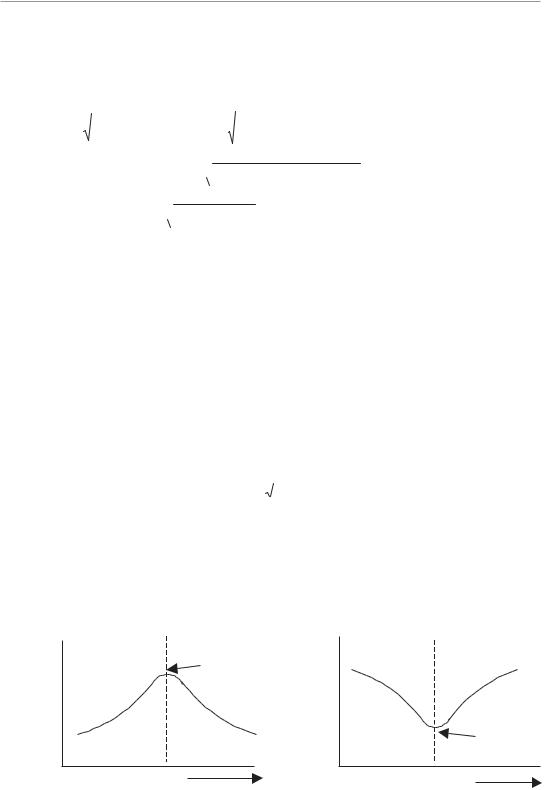
When the input frequency is below the resonant frequency XC is larger than XL, and the circuit is capacitive; above the resonant frequency, XL is larger than XC, and the circuit is inductive. Plotting the input current against the input frequency shows a peak in the input current at the resonant frequency, as shown in Figure 3.5(a).
|
Resonant |
Supplycurrent |
frequency |
|
|
|
Frequency |
|
(a) |
current |
|
|
Supply |
Resonant |
|
frequency |
||
|
||
|
Frequency |
|
|
(b) |
Figure 3.5 Supply current versus frequency in (a) series circuit, and (b) parallel circuit.
www.globalautomation.info
3.2 Circuits with R, L, and C |
31 |
Example 3.4
What is the resonant frequency of the series circuit in Figure 3.3(a)? What is the current at this frequency? Assume the same values as in Example 3.3.
Using Equation (3.9), we get:
f = |
|
|
1 |
|
Hz = |
|
|
|
|
1 |
|
Hz |
||
2π |
|
|
|
|
|
|
|
|
|
|
||||
|
LC |
2 × 3142. × |
2.2 × 10−9 × 33 × 10−3 |
|||||||||||
|
|
|
|
|
|
|||||||||
f = |
|
|
|
|
1 |
|
Hz = |
106 |
|
Hz = 187. × 104 Hz |
||||
|
|
|
|
|
|
|
|
|
||||||
2 |
× 3142. × 8.5 × 10⁻⁶ |
53.4 |
|
|
||||||||||
f = 187.kHz
The current can be obtained using Equation 3.7, at resonance Z = R.
I = E/Z = 20/18.7 × 103 = 1.07 mA
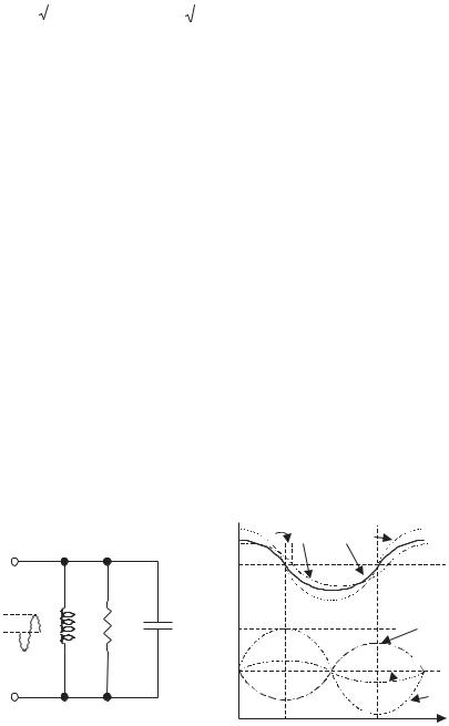
When R, L, and C are connected in parallel, as shown in Figure 3.6(a), each component will see the same voltage but not the same current, as shown by the waveforms in Figure 3.6(b).
The source current (IS) is the vector sum of the currents in each component, and is given by:
IS |
2 = IR |
2 + (IL − IC )2 |
(3.10) |
The impedance of the circuit (Z) as seen by the input is given by:
1 |
= |
1 |
+ |
1 |
(3.11) |
|
Z2 |
R2 |
|
(XL − XC )2 |
|||
At the resonant frequency, IL and IC become equal and cancel, and the current (I) is given by:
θ |
IR |
I E |
AC input |
E |
L |
R |
|
IC |
|
C |
||||
|
|
|
|
IC |
|
|
|
|
|
|
 + IL
+ IL
IL
90° 180° 270° Time
(a) |
(b) |
Figure 3.6 (a) Parallel R, C, and L circuits, and (b) waveforms and phase relations in a parallel circuit.
www.globalautomation.info
32 |
Basic Electrical Components |
I = IL = IC = V × 2πfC = V 2πfL |
(3.12) |
Thus, at resonance, E = IR, as seen from (3.10). Below the resonant frequency, the circuit is inductive, and above the resonant frequency, the circuit is capacitive. Plotting the current against frequency shows the current is a minimum at the resonant frequency, as shown in the frequency plot in Figure 3.5(b). The frequency at resonance is given by (3.9), and the current is given by (3.7).
3.3RC Filters
Passive networks using resistors and capacitors are extensively used [2], and sometimes small inductors are used in instrumentation circuits for filtering out noise, frequency selection, and frequency rejection, and so forth. Filters can be either passive
[3]or active (using amplifiers), and are divided into the following types.
•High-pass. Allows high frequencies to pass but blocks low frequencies;
•Low-pass. Allows low frequencies to pass but blocks high frequencies;
•Band-pass. Allows a specific range of frequencies to pass;
•Band reject. Blocks a specific range of frequencies;
•Twin – T. Form of band reject filter, but with a sharper response characteristic.
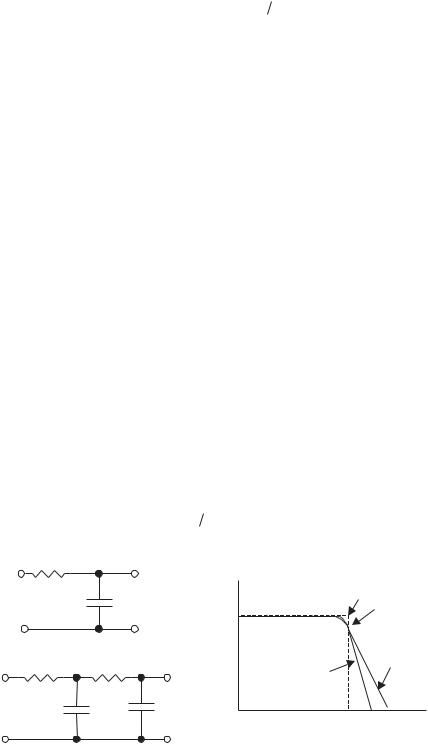
Figure 3.7(a) shows a first order and second order low-pass RC filter [4], which passes low frequencies and rejects high frequencies, as shown in the frequency response curve in Figure 3.7(b). The cutoff frequency (fc) of a filter is defined as the frequency at which the output power is reduced to one-half of the input power (−3 dB, or the output voltage is 0.707Vin). In the case of the first order low-pass filter, the cutoff frequency is given by:
fc = 1 2πRC |
(3.13) |
|
R |
C |
Vin |
|
|
|
Vout |
R1 R2
Vin |
C1 |
C2 |
Vout |
(a)
Voltage gain (dB)
|
Ideal |
|
0 |
−3 dB |
|
|
||
−10 |
1st Order |
|
6 dB/Octave |
||
|
20 dB/Decade |
|
−20 |
2nd Order |
|
12 dB/Octave |
||
|
||
|
40 dB/Decade |
|
−30 |
|
|
1 |
10 100 1 kfc 10 kf |
|
|
Frequency |
(b)
Figure 3.7 (a) First order and second order low-pass filters, and (b) gain-frequency characteristics of first order and second order filters.
www.globalautomation.info
3.3 RC Filters |
33 |
In the case of the second order low-pass filter, the cutoff frequency is given by:
fc |
= |
|
1 |
|
Hz |
(3.14) |
|
2π |
|
|
|||||
R1R2 C1C2 |
|||||||
|
|
|
|
|
The output voltage drops off at 20 dB/decade with a first order filter, 40 dB/decade for a second order filter, 60 dB/decade for a third order filter, and so forth. There is also a phase change associated with filters: −45° for a first order filter, −90° for a second order filter, −135° for a third order filter, and so forth. The phase change can cause instability in active circuits [5].
The input to output voltage ratio for any frequency (f) for a first order low-pass filter is given by:
Vout |
1 |
|
|
|
= |
|
(3.15) |
Vin |
[1+ (f fc )2 ]1 2 |
||
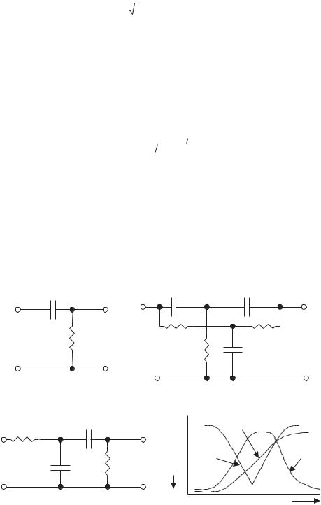
The circuit for a high-pass, band-pass, and twin-T passive filters are shown in Figure 3.8. The number of resistive and capacitive elements determines the order of the filter (e.g., first order, second order, and so forth). The circuit configuration determines the characteristics of the filters, such as Butterworth, Bessel, Chebyshev, and Legendre. Figure 3.8(d) shows the frequency characteristics of the filters shown in Figure 3.8(a–c) [6].
These are examples of the use of resistors and capacitors in RC networks. Further descriptions of filters can be found in electronic textbooks [7].
C |
|
|
|
C |
C |
|
|
|
|
|
|
||
|
|
|
|
|
|
|
Vin |
|
Vout |
|
R |
R |
|
R |
|
|
|
Vout |
||
|
|
Vin |
|
R |
||
|
|
|
|
|
||
|
|
|
|
|
C |
|
(a) |
|
|
|
|
(c) |
|
RL |
CH |
|
|
|
Low pass |
|
|
|
|
|
|
||
|
|
|
|
|
|
|
CL |
|
|
|
(dB) |
Twin −T |
Band pass |
|
R |
|
Gain |
|||
|
Vout |
|
||||
Vin |
|
H |
|
|
||
|
|
|
|
|||
|
|
|
|
|
|
|
|
|
|
|
|
Frequency |
|
(b) |
|
|
|
|
(d) |
|
Figure 3.8 (a) High-pass filters, (b) band-pass filters, (c) twin-T band reject filters, and (d) their frequency characteristics.
|
www.globalautomation.info |
34 |
Basic Electrical Components |
3.4Bridge Circuits
Resistor temperature compensation can be achieved in voltage divider circuits or bridge circuits. However, when trying to measure small changes in resistance, as required in strain gauges (see Section 11.3.4), the signal resolution in bridge circuits is much higher than with voltage dividers. Bridge circuits are used to convert small changes in impedance into voltages. These voltages are referenced to zero, so that the signals can be amplified to give high sensitivity to impedance changes.
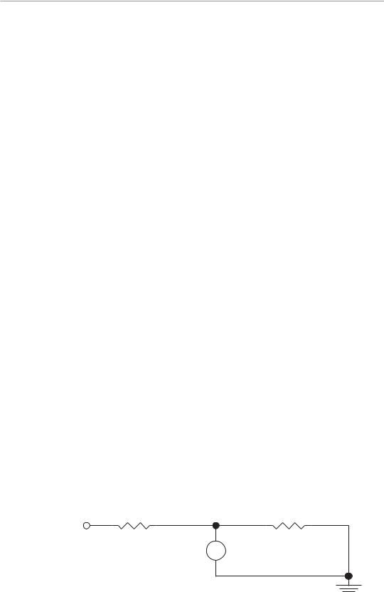
3.4.1Voltage Dividers
The two resistive elements R1 and R2 in a strain gauge sensor can be connected in series to form a voltage divider, as shown in Figure 3.9. The elements are driven from a supply, Vs. Since the temperature coefficient of resistance is the same in both elements, the voltage at the junction of the elements, VR, is independent of temperature, and is given by:
VR |
= |
|
R2 VS |
(3.16) |
||
R1 |
+ R2 |
|||||
|
|
|
||||
Example 3.5
The resistive elements in a strain gauge are each 5kΩ. A digital voltmeter with ranges of 10V, 1V, and 0.1V, and a resolution of 0.1% of FSD, is used to measure the output voltage. If R2 is the fixed element and R1 is the element measuring strain, what is the minimum change in R1 that can be detected? Assume a supply of 10V.
To measure the output voltage ≈ 5V, the 10V range is required, giving a resolution or sensitivity of 10 mV.
VR = 5.01V = 5,000 × 10/(R1 + 5,000)V
5.01(R1 + 5,000) = 50,000
R1 = (50,000/5.01) − 5,000 = 4,980Ω
Resolution = 5,000 − 4,980 = 20Ω
3.4.2dc Bridge Circuits
The simplest and most common bridge network is the DC Wheatstone bridge. The basic bridge is shown in Figure 3.10; this bridge is used in sensor applications, where small changes in resistance are to be measured. The basic bridge is modified for use in many other specific applications. In the basic bridge four resistors are connected
R1 |
R2 |
Vs
+
VR V
−
Figure 3.9 Voltage divider.