- •Preface
- •Imaging Microscopic Features
- •Measuring the Crystal Structure
- •References
- •Contents
- •1.4 Simulating the Effects of Elastic Scattering: Monte Carlo Calculations
- •What Are the Main Features of the Beam Electron Interaction Volume?
- •How Does the Interaction Volume Change with Composition?
- •How Does the Interaction Volume Change with Incident Beam Energy?
- •How Does the Interaction Volume Change with Specimen Tilt?
- •1.5 A Range Equation To Estimate the Size of the Interaction Volume
- •References
- •2: Backscattered Electrons
- •2.1 Origin
- •2.2.1 BSE Response to Specimen Composition (η vs. Atomic Number, Z)
- •SEM Image Contrast with BSE: “Atomic Number Contrast”
- •SEM Image Contrast: “BSE Topographic Contrast—Number Effects”
- •2.2.3 Angular Distribution of Backscattering
- •Beam Incident at an Acute Angle to the Specimen Surface (Specimen Tilt > 0°)
- •SEM Image Contrast: “BSE Topographic Contrast—Trajectory Effects”
- •2.2.4 Spatial Distribution of Backscattering
- •Depth Distribution of Backscattering
- •Radial Distribution of Backscattered Electrons
- •2.3 Summary
- •References
- •3: Secondary Electrons
- •3.1 Origin
- •3.2 Energy Distribution
- •3.3 Escape Depth of Secondary Electrons
- •3.8 Spatial Characteristics of Secondary Electrons
- •References
- •4: X-Rays
- •4.1 Overview
- •4.2 Characteristic X-Rays
- •4.2.1 Origin
- •4.2.2 Fluorescence Yield
- •4.2.3 X-Ray Families
- •4.2.4 X-Ray Nomenclature
- •4.2.6 Characteristic X-Ray Intensity
- •Isolated Atoms
- •X-Ray Production in Thin Foils
- •X-Ray Intensity Emitted from Thick, Solid Specimens
- •4.3 X-Ray Continuum (bremsstrahlung)
- •4.3.1 X-Ray Continuum Intensity
- •4.3.3 Range of X-ray Production
- •4.4 X-Ray Absorption
- •4.5 X-Ray Fluorescence
- •References
- •5.1 Electron Beam Parameters
- •5.2 Electron Optical Parameters
- •5.2.1 Beam Energy
- •Landing Energy
- •5.2.2 Beam Diameter
- •5.2.3 Beam Current
- •5.2.4 Beam Current Density
- •5.2.5 Beam Convergence Angle, α
- •5.2.6 Beam Solid Angle
- •5.2.7 Electron Optical Brightness, β
- •Brightness Equation
- •5.2.8 Focus
- •Astigmatism
- •5.3 SEM Imaging Modes
- •5.3.1 High Depth-of-Field Mode
- •5.3.2 High-Current Mode
- •5.3.3 Resolution Mode
- •5.3.4 Low-Voltage Mode
- •5.4 Electron Detectors
- •5.4.1 Important Properties of BSE and SE for Detector Design and Operation
- •Abundance
- •Angular Distribution
- •Kinetic Energy Response
- •5.4.2 Detector Characteristics
- •Angular Measures for Electron Detectors
- •Elevation (Take-Off) Angle, ψ, and Azimuthal Angle, ζ
- •Solid Angle, Ω
- •Energy Response
- •Bandwidth
- •5.4.3 Common Types of Electron Detectors
- •Backscattered Electrons
- •Passive Detectors
- •Scintillation Detectors
- •Semiconductor BSE Detectors
- •5.4.4 Secondary Electron Detectors
- •Everhart–Thornley Detector
- •Through-the-Lens (TTL) Electron Detectors
- •TTL SE Detector
- •TTL BSE Detector
- •Measuring the DQE: BSE Semiconductor Detector
- •References
- •6: Image Formation
- •6.1 Image Construction by Scanning Action
- •6.2 Magnification
- •6.3 Making Dimensional Measurements With the SEM: How Big Is That Feature?
- •Using a Calibrated Structure in ImageJ-Fiji
- •6.4 Image Defects
- •6.4.1 Projection Distortion (Foreshortening)
- •6.4.2 Image Defocusing (Blurring)
- •6.5 Making Measurements on Surfaces With Arbitrary Topography: Stereomicroscopy
- •6.5.1 Qualitative Stereomicroscopy
- •Fixed beam, Specimen Position Altered
- •Fixed Specimen, Beam Incidence Angle Changed
- •6.5.2 Quantitative Stereomicroscopy
- •Measuring a Simple Vertical Displacement
- •References
- •7: SEM Image Interpretation
- •7.1 Information in SEM Images
- •7.2.2 Calculating Atomic Number Contrast
- •Establishing a Robust Light-Optical Analogy
- •Getting It Wrong: Breaking the Light-Optical Analogy of the Everhart–Thornley (Positive Bias) Detector
- •Deconstructing the SEM/E–T Image of Topography
- •SUM Mode (A + B)
- •DIFFERENCE Mode (A−B)
- •References
- •References
- •9: Image Defects
- •9.1 Charging
- •9.1.1 What Is Specimen Charging?
- •9.1.3 Techniques to Control Charging Artifacts (High Vacuum Instruments)
- •Observing Uncoated Specimens
- •Coating an Insulating Specimen for Charge Dissipation
- •Choosing the Coating for Imaging Morphology
- •9.2 Radiation Damage
- •9.3 Contamination
- •References
- •10: High Resolution Imaging
- •10.2 Instrumentation Considerations
- •10.4.1 SE Range Effects Produce Bright Edges (Isolated Edges)
- •10.4.4 Too Much of a Good Thing: The Bright Edge Effect Hinders Locating the True Position of an Edge for Critical Dimension Metrology
- •10.5.1 Beam Energy Strategies
- •Low Beam Energy Strategy
- •High Beam Energy Strategy
- •Making More SE1: Apply a Thin High-δ Metal Coating
- •Making Fewer BSEs, SE2, and SE3 by Eliminating Bulk Scattering From the Substrate
- •10.6 Factors That Hinder Achieving High Resolution
- •10.6.2 Pathological Specimen Behavior
- •Contamination
- •Instabilities
- •References
- •11: Low Beam Energy SEM
- •11.3 Selecting the Beam Energy to Control the Spatial Sampling of Imaging Signals
- •11.3.1 Low Beam Energy for High Lateral Resolution SEM
- •11.3.2 Low Beam Energy for High Depth Resolution SEM
- •11.3.3 Extremely Low Beam Energy Imaging
- •References
- •12.1.1 Stable Electron Source Operation
- •12.1.2 Maintaining Beam Integrity
- •12.1.4 Minimizing Contamination
- •12.3.1 Control of Specimen Charging
- •12.5 VPSEM Image Resolution
- •References
- •13: ImageJ and Fiji
- •13.1 The ImageJ Universe
- •13.2 Fiji
- •13.3 Plugins
- •13.4 Where to Learn More
- •References
- •14: SEM Imaging Checklist
- •14.1.1 Conducting or Semiconducting Specimens
- •14.1.2 Insulating Specimens
- •14.2 Electron Signals Available
- •14.2.1 Beam Electron Range
- •14.2.2 Backscattered Electrons
- •14.2.3 Secondary Electrons
- •14.3 Selecting the Electron Detector
- •14.3.2 Backscattered Electron Detectors
- •14.3.3 “Through-the-Lens” Detectors
- •14.4 Selecting the Beam Energy for SEM Imaging
- •14.4.4 High Resolution SEM Imaging
- •Strategy 1
- •Strategy 2
- •14.5 Selecting the Beam Current
- •14.5.1 High Resolution Imaging
- •14.5.2 Low Contrast Features Require High Beam Current and/or Long Frame Time to Establish Visibility
- •14.6 Image Presentation
- •14.6.1 “Live” Display Adjustments
- •14.6.2 Post-Collection Processing
- •14.7 Image Interpretation
- •14.7.1 Observer’s Point of View
- •14.7.3 Contrast Encoding
- •14.8.1 VPSEM Advantages
- •14.8.2 VPSEM Disadvantages
- •15: SEM Case Studies
- •15.1 Case Study: How High Is That Feature Relative to Another?
- •15.2 Revealing Shallow Surface Relief
- •16.1.2 Minor Artifacts: The Si-Escape Peak
- •16.1.3 Minor Artifacts: Coincidence Peaks
- •16.1.4 Minor Artifacts: Si Absorption Edge and Si Internal Fluorescence Peak
- •16.2 “Best Practices” for Electron-Excited EDS Operation
- •16.2.1 Operation of the EDS System
- •Choosing the EDS Time Constant (Resolution and Throughput)
- •Choosing the Solid Angle of the EDS
- •Selecting a Beam Current for an Acceptable Level of System Dead-Time
- •16.3.1 Detector Geometry
- •16.3.2 Process Time
- •16.3.3 Optimal Working Distance
- •16.3.4 Detector Orientation
- •16.3.5 Count Rate Linearity
- •16.3.6 Energy Calibration Linearity
- •16.3.7 Other Items
- •16.3.8 Setting Up a Quality Control Program
- •Using the QC Tools Within DTSA-II
- •Creating a QC Project
- •Linearity of Output Count Rate with Live-Time Dose
- •Resolution and Peak Position Stability with Count Rate
- •Solid Angle for Low X-ray Flux
- •Maximizing Throughput at Moderate Resolution
- •References
- •17: DTSA-II EDS Software
- •17.1 Getting Started With NIST DTSA-II
- •17.1.1 Motivation
- •17.1.2 Platform
- •17.1.3 Overview
- •17.1.4 Design
- •Simulation
- •Quantification
- •Experiment Design
- •Modeled Detectors (. Fig. 17.1)
- •Window Type (. Fig. 17.2)
- •The Optimal Working Distance (. Figs. 17.3 and 17.4)
- •Elevation Angle
- •Sample-to-Detector Distance
- •Detector Area
- •Crystal Thickness
- •Number of Channels, Energy Scale, and Zero Offset
- •Resolution at Mn Kα (Approximate)
- •Azimuthal Angle
- •Gold Layer, Aluminum Layer, Nickel Layer
- •Dead Layer
- •Zero Strobe Discriminator (. Figs. 17.7 and 17.8)
- •Material Editor Dialog (. Figs. 17.9, 17.10, 17.11, 17.12, 17.13, and 17.14)
- •17.2.1 Introduction
- •17.2.2 Monte Carlo Simulation
- •17.2.4 Optional Tables
- •References
- •18: Qualitative Elemental Analysis by Energy Dispersive X-Ray Spectrometry
- •18.1 Quality Assurance Issues for Qualitative Analysis: EDS Calibration
- •18.2 Principles of Qualitative EDS Analysis
- •Exciting Characteristic X-Rays
- •Fluorescence Yield
- •X-ray Absorption
- •Si Escape Peak
- •Coincidence Peaks
- •18.3 Performing Manual Qualitative Analysis
- •Beam Energy
- •Choosing the EDS Resolution (Detector Time Constant)
- •Obtaining Adequate Counts
- •18.4.1 Employ the Available Software Tools
- •18.4.3 Lower Photon Energy Region
- •18.4.5 Checking Your Work
- •18.5 A Worked Example of Manual Peak Identification
- •References
- •19.1 What Is a k-ratio?
- •19.3 Sets of k-ratios
- •19.5 The Analytical Total
- •19.6 Normalization
- •19.7.1 Oxygen by Assumed Stoichiometry
- •19.7.3 Element by Difference
- •19.8 Ways of Reporting Composition
- •19.8.1 Mass Fraction
- •19.8.2 Atomic Fraction
- •19.8.3 Stoichiometry
- •19.8.4 Oxide Fractions
- •Example Calculations
- •19.9 The Accuracy of Quantitative Electron-Excited X-ray Microanalysis
- •19.9.1 Standards-Based k-ratio Protocol
- •19.9.2 “Standardless Analysis”
- •19.10 Appendix
- •19.10.1 The Need for Matrix Corrections To Achieve Quantitative Analysis
- •19.10.2 The Physical Origin of Matrix Effects
- •19.10.3 ZAF Factors in Microanalysis
- •X-ray Generation With Depth, φ(ρz)
- •X-ray Absorption Effect, A
- •X-ray Fluorescence, F
- •References
- •20.2 Instrumentation Requirements
- •20.2.1 Choosing the EDS Parameters
- •EDS Spectrum Channel Energy Width and Spectrum Energy Span
- •EDS Time Constant (Resolution and Throughput)
- •EDS Calibration
- •EDS Solid Angle
- •20.2.2 Choosing the Beam Energy, E0
- •20.2.3 Measuring the Beam Current
- •20.2.4 Choosing the Beam Current
- •Optimizing Analysis Strategy
- •20.3.4 Ba-Ti Interference in BaTiSi3O9
- •20.4 The Need for an Iterative Qualitative and Quantitative Analysis Strategy
- •20.4.2 Analysis of a Stainless Steel
- •20.5 Is the Specimen Homogeneous?
- •20.6 Beam-Sensitive Specimens
- •20.6.1 Alkali Element Migration
- •20.6.2 Materials Subject to Mass Loss During Electron Bombardment—the Marshall-Hall Method
- •Thin Section Analysis
- •Bulk Biological and Organic Specimens
- •References
- •21: Trace Analysis by SEM/EDS
- •21.1 Limits of Detection for SEM/EDS Microanalysis
- •21.2.1 Estimating CDL from a Trace or Minor Constituent from Measuring a Known Standard
- •21.2.2 Estimating CDL After Determination of a Minor or Trace Constituent with Severe Peak Interference from a Major Constituent
- •21.3 Measurements of Trace Constituents by Electron-Excited Energy Dispersive X-ray Spectrometry
- •The Inevitable Physics of Remote Excitation Within the Specimen: Secondary Fluorescence Beyond the Electron Interaction Volume
- •Simulation of Long-Range Secondary X-ray Fluorescence
- •NIST DTSA II Simulation: Vertical Interface Between Two Regions of Different Composition in a Flat Bulk Target
- •NIST DTSA II Simulation: Cubic Particle Embedded in a Bulk Matrix
- •21.5 Summary
- •References
- •22.1.2 Low Beam Energy Analysis Range
- •22.2 Advantage of Low Beam Energy X-Ray Microanalysis
- •22.2.1 Improved Spatial Resolution
- •22.3 Challenges and Limitations of Low Beam Energy X-Ray Microanalysis
- •22.3.1 Reduced Access to Elements
- •22.3.3 At Low Beam Energy, Almost Everything Is Found To Be Layered
- •Analysis of Surface Contamination
- •References
- •23: Analysis of Specimens with Special Geometry: Irregular Bulk Objects and Particles
- •23.2.1 No Chemical Etching
- •23.3 Consequences of Attempting Analysis of Bulk Materials With Rough Surfaces
- •23.4.1 The Raw Analytical Total
- •23.4.2 The Shape of the EDS Spectrum
- •23.5 Best Practices for Analysis of Rough Bulk Samples
- •23.6 Particle Analysis
- •Particle Sample Preparation: Bulk Substrate
- •The Importance of Beam Placement
- •Overscanning
- •“Particle Mass Effect”
- •“Particle Absorption Effect”
- •The Analytical Total Reveals the Impact of Particle Effects
- •Does Overscanning Help?
- •23.6.6 Peak-to-Background (P/B) Method
- •Specimen Geometry Severely Affects the k-ratio, but Not the P/B
- •Using the P/B Correspondence
- •23.7 Summary
- •References
- •24: Compositional Mapping
- •24.2 X-Ray Spectrum Imaging
- •24.2.1 Utilizing XSI Datacubes
- •24.2.2 Derived Spectra
- •SUM Spectrum
- •MAXIMUM PIXEL Spectrum
- •24.3 Quantitative Compositional Mapping
- •24.4 Strategy for XSI Elemental Mapping Data Collection
- •24.4.1 Choosing the EDS Dead-Time
- •24.4.2 Choosing the Pixel Density
- •24.4.3 Choosing the Pixel Dwell Time
- •“Flash Mapping”
- •High Count Mapping
- •References
- •25.1 Gas Scattering Effects in the VPSEM
- •25.1.1 Why Doesn’t the EDS Collimator Exclude the Remote Skirt X-Rays?
- •25.2 What Can Be Done To Minimize gas Scattering in VPSEM?
- •25.2.2 Favorable Sample Characteristics
- •Particle Analysis
- •25.2.3 Unfavorable Sample Characteristics
- •References
- •26.1 Instrumentation
- •26.1.2 EDS Detector
- •26.1.3 Probe Current Measurement Device
- •Direct Measurement: Using a Faraday Cup and Picoammeter
- •A Faraday Cup
- •Electrically Isolated Stage
- •Indirect Measurement: Using a Calibration Spectrum
- •26.1.4 Conductive Coating
- •26.2 Sample Preparation
- •26.2.1 Standard Materials
- •26.2.2 Peak Reference Materials
- •26.3 Initial Set-Up
- •26.3.1 Calibrating the EDS Detector
- •Selecting a Pulse Process Time Constant
- •Energy Calibration
- •Quality Control
- •Sample Orientation
- •Detector Position
- •Probe Current
- •26.4 Collecting Data
- •26.4.1 Exploratory Spectrum
- •26.4.2 Experiment Optimization
- •26.4.3 Selecting Standards
- •26.4.4 Reference Spectra
- •26.4.5 Collecting Standards
- •26.4.6 Collecting Peak-Fitting References
- •26.5 Data Analysis
- •26.5.2 Quantification
- •26.6 Quality Check
- •Reference
- •27.2 Case Study: Aluminum Wire Failures in Residential Wiring
- •References
- •28: Cathodoluminescence
- •28.1 Origin
- •28.2 Measuring Cathodoluminescence
- •28.3 Applications of CL
- •28.3.1 Geology
- •Carbonado Diamond
- •Ancient Impact Zircons
- •28.3.2 Materials Science
- •Semiconductors
- •Lead-Acid Battery Plate Reactions
- •28.3.3 Organic Compounds
- •References
- •29.1.1 Single Crystals
- •29.1.2 Polycrystalline Materials
- •29.1.3 Conditions for Detecting Electron Channeling Contrast
- •Specimen Preparation
- •Instrument Conditions
- •29.2.1 Origin of EBSD Patterns
- •29.2.2 Cameras for EBSD Pattern Detection
- •29.2.3 EBSD Spatial Resolution
- •29.2.5 Steps in Typical EBSD Measurements
- •Sample Preparation for EBSD
- •Align Sample in the SEM
- •Check for EBSD Patterns
- •Adjust SEM and Select EBSD Map Parameters
- •Run the Automated Map
- •29.2.6 Display of the Acquired Data
- •29.2.7 Other Map Components
- •29.2.10 Application Example
- •Application of EBSD To Understand Meteorite Formation
- •29.2.11 Summary
- •Specimen Considerations
- •EBSD Detector
- •Selection of Candidate Crystallographic Phases
- •Microscope Operating Conditions and Pattern Optimization
- •Selection of EBSD Acquisition Parameters
- •Collect the Orientation Map
- •References
- •30.1 Introduction
- •30.2 Ion–Solid Interactions
- •30.3 Focused Ion Beam Systems
- •30.5 Preparation of Samples for SEM
- •30.5.1 Cross-Section Preparation
- •30.5.2 FIB Sample Preparation for 3D Techniques and Imaging
- •30.6 Summary
- •References
- •31: Ion Beam Microscopy
- •31.1 What Is So Useful About Ions?
- •31.2 Generating Ion Beams
- •31.3 Signal Generation in the HIM
- •31.5 Patterning with Ion Beams
- •31.7 Chemical Microanalysis with Ion Beams
- •References
- •Appendix
- •A Database of Electron–Solid Interactions
- •Introduction
- •Backscattered Electrons
- •Secondary Yields
- •Stopping Powers
- •X-ray Ionization Cross Sections
- •Conclusions
- •References
- •Index
- •Reference List
- •Index
2.2 · Critical Properties of Backscattered Electrons
seen in . Fig. 2.9b, with this distribution measured for a tilt of 60° (angle of incidence = 30°). The angular distribution is peaked in the forward direction away from the incident beam direction, with the maximum BSE emission occurring at an angle above the surface close to the value of the angle of incidence above the surface of the beam. This angular asymmetry develops slowly for tilt angles up to approximately 30°, but the asymmetry becomes increasingly pronounced with further increases in the specimen tilt. Moreover, the rotational symmetry of the 0° tilt case is also progressively lost with increasing tilt, with the asymmetric distribution seen in . Fig. 2.9b becoming much narrower in the direction out of the plotting plane. See 7 Chapter 29 for effects of crystal structure on backscattering angular distribution.
SEM Image Contrast: “BSE Topographic Contrast—Trajectory Effects”
The overall effects of specimen tilt are to increase the number of backscattered electrons and to create directionality in the backscattered electron emission, and both effects become increasingly stronger as the tilt increases. The “trajectory effects” create a very strong component of topographic contrast when viewed with a backscattered electron detector that has limited size and is placed preferentially on one side of the specimen. . Figure 2.8b shows the same area as . Fig. 2.8a imaged with a small solid angle detector, located at the top center of the image. Very strong contrast is created between faces tilted toward the detector, i.e., facing upward, and those tilted away, i.e., facing downward. These effects will be discussed in detail in the Image Interpretation module.
23 |
|
2 |
|
|
|
2.2.4\ Spatial Distribution of Backscattering
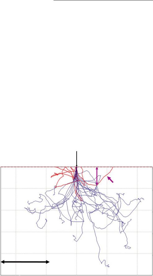
Model a small number of trajectories (~25) so that the individual trajectories can be distinguished; e.g., for a copper target with an incident beam energy of 20 keV and 0° tilt, as seen in
. Fig. 2.10 (Note: because of the random number sampling, repeated simulations will differ from each other and will be different from the printed example.) By following a number of trajectories from the point of incidence to the point of escape through the surface as backscattered electrons, it can be seen that the trajectories of beam electrons that eventually emerge as BSEs typically traverse the specimen both laterally and in depth.
Depth Distribution of Backscattering
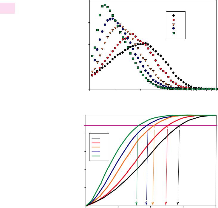
By performing detailed Monte Carlo simulations for many thousands of trajectories and recording for each trajectory the maximum depth of penetration into the specimen before the electron eventually escaped as a BSE, we can determine the contribution to the overall backscatter coefficient as a function of the depth of penetration, as shown for a series of elements in . Fig. 2.11a. To compare the different elements, the horizontal axis of the plot is the depth normalized by the Kanaya–Okayama range for each element. From the depth distribution data in . Fig. 2.11a, the cumulative backscattering coefficient as a function of depth can be calculated, and as shown in . Fig. 2.11b, this distribution follows an S-shaped curve. To capture 90 % of the total backscattering, which corresponds to the region where the slope of the plot is rapidly decreasing, the backscattered electrons are found to travel a
. Fig. 2.10 Monte Carlo simulation of a few trajectories in copper with an incident beam energy of 20 keV and 0° tilt to show effect of penetration depth of backscattered electrons
Cu
Cu
E0 = 20 keV 0º tilt
500 nm
Maximum |
0.0 nm |
depth of penetration for this trajectory
leading to BSE. 219.7 nm
439.5 nm
659.2 nm
878.9 nm
-640.0 nm |
-320.0 nm |
-0.0 nm |
320.0 nm |
640.0 nm |
24\ Chapter 2 · Backscattered Electrons
|
. Fig. 2.11 a Distribution |
|
of depth penetration of back- |
|
scattered electrons in various |
2 |
elements. b Cumulative backscat- |
tering coefficient as a function |
of the depth of penetration in various elements, showing determination of 90 % total backscattering depth
a
Backscatter fraction
Backscattered electron penetration
0.08
|
C |
|
0.06 |
AI |
|
Cu |
||
|
||
|
Ag |
|
|
Au |
|
0.04 |
|
0.02
0.00 |
|
|
|
|
|
0.0 |
0.1 |
0.2 |
0.3 |
0.4 |
0.5 |
|
|
Depth/range (Kanaya-Okayama) |
|
|
b
Cumulative backscattering (normalized)
1.0
0.8
0.6
0.4
0.2
0.0
0.0
Backscattering vs. depth
C
AI
Cu
Ag
Au
0.155 |
0.185 |
0.205 |
0.250 |
0.285 |
|
0.1 |
|
0.2 |
|
0.3 |
0.4 |
Depth/range (Kanaya-Okayama) |
|
|
significant fraction of the Kanaya–Okayama range into the target. Strong elastic scattering materials with high atomic number such as gold sample a smaller fraction of the range than the weak elastic scattering materials such as carbon.
. Table 2.2 lists the fractional range to capture 90 % of backscattering at normal beam incidence (0° tilt) and for a similar
Monte Carlo study performed for a target at 45° tilt. For a tilted target, all materials show a slightly smaller fraction of the Kanaya–Okayama range to reach 90 % backscattering compared to the normal incidence case.
When the beam energy is increased for a specific material, the strong dependence of the total range on the incident
2.2 · Critical Properties of Backscattered Electrons
. Table 2.2 BSE penetration depth (D/RK-O) to capture 90 % of
total backscattering
|
0º tilt |
45º tilt |
|
|
|
C |
0.285 |
0.23 |
|
|
|
Al |
0.250 |
0.21 |
Cu |
0.205 |
0.19 |
Ag |
0.185 |
0.17 |
Au |
0.155 |
0.15 |
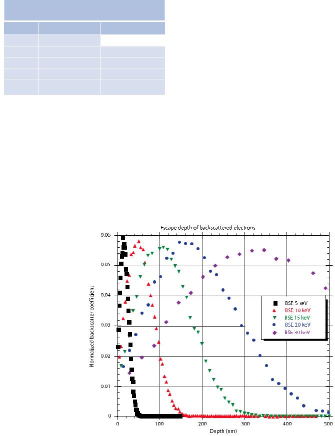
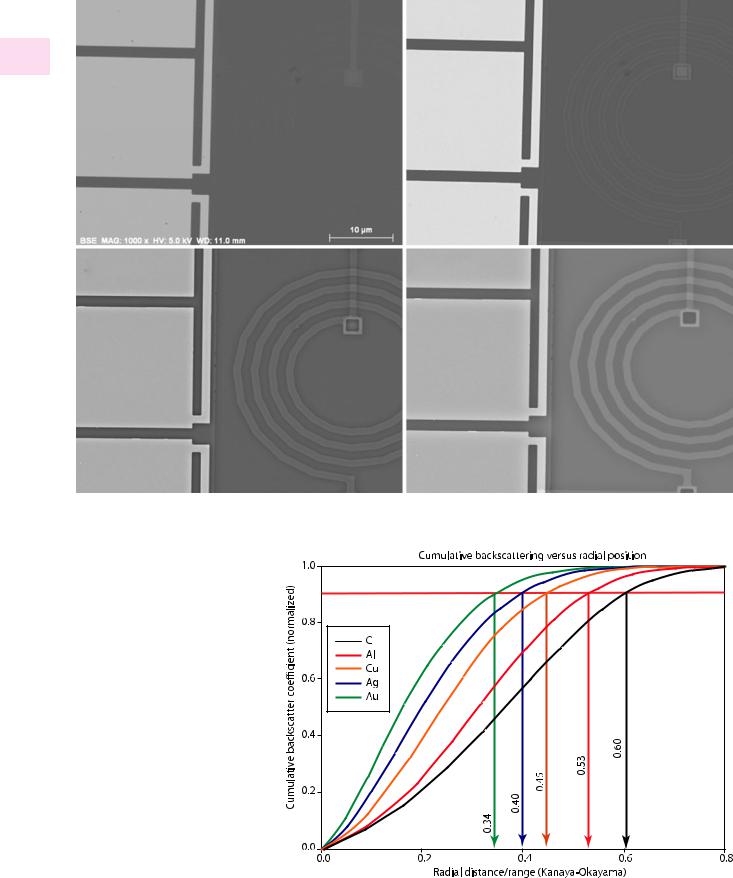
beam energy leads to a strong dependence of the sampling depth of backscattered electrons, as shown in the depth distributions of backscattered electrons for copper over a wide energy range in . Fig. 2.12. The substantial sampling depth of backscattered electrons combined with the strong dependence of the electron range on beam energy provides a useful tool for the microscopist. By comparing a series of images of a given area as a function of beam energy, subsurface details can be recognized. An example is shown in . Fig. 2.13 for an engineered semiconductor electronic device with three- dimensional layered features, where a systematic increase in the beam energy reveals progressively deeper structures.
25 |
|
2 |
|
|
|
Radial Distribution of Backscattered Electrons
The Monte Carlo simulation can record the x-y location at which a backscattered electron exits through the surface plane, and this information can be used to calculate the radial distribution of backscattering relative to the beam impact location. The cumulative radial distribution is shown in . Fig. 2.14 for a series of elements, as normalized by the Kanaya–Okayama range for each element, and an S-shaped curve is observed. . Table 2.3 gives the fraction of the range necessary to capture 90 % of the total backscattering. The radial distribution is steepest for high atomic number elements, which scatter strongly compared to weakly scattering low atomic number elements. However, even for strongly scattering elements, the backscattered electrons emerge over a significant fraction of the range. This characteristic impacts the spatial resolution that can be obtained with backscattered electron images. An example is shown in . Fig. 2.15 for an interface between an aluminum-rich phase and a copper- rich phase (CuAl2) in directionally solidified aluminum- copper eutectic alloy. The interfaces are perpendicular to the surface and are atomically sharp. The backscattered electron signal response as the beam is scanned across the interface is more than an order-of-magnitude broader (~300 nm) due to the lateral spreading of backscattering than would be predicted from the incident beam diameter alone (10 nm).
. Fig. 2.12 Backscattered electron depth distributions at various energies in copper at 0° tilt
\26 Chapter 2 · Backscattered Electrons
5 keV |
10 keV |
2
20 keV |
30 keV |
. Fig. 2.13 BSE images at various incident beam energies of a semiconductor device consisting of silicon and various metallization layers at different depths
. Fig. 2.14 Cumulative radial distribution of backscattered electrons in various bulk pure elements at 0° tilt showing determination of 90 % total backscattering radius