

- •Preface
- •Imaging Microscopic Features
- •Measuring the Crystal Structure
- •References
- •Contents
- •1.4 Simulating the Effects of Elastic Scattering: Monte Carlo Calculations
- •What Are the Main Features of the Beam Electron Interaction Volume?
- •How Does the Interaction Volume Change with Composition?
- •How Does the Interaction Volume Change with Incident Beam Energy?
- •How Does the Interaction Volume Change with Specimen Tilt?
- •1.5 A Range Equation To Estimate the Size of the Interaction Volume
- •References
- •2: Backscattered Electrons
- •2.1 Origin
- •2.2.1 BSE Response to Specimen Composition (η vs. Atomic Number, Z)
- •SEM Image Contrast with BSE: “Atomic Number Contrast”
- •SEM Image Contrast: “BSE Topographic Contrast—Number Effects”
- •2.2.3 Angular Distribution of Backscattering
- •Beam Incident at an Acute Angle to the Specimen Surface (Specimen Tilt > 0°)
- •SEM Image Contrast: “BSE Topographic Contrast—Trajectory Effects”
- •2.2.4 Spatial Distribution of Backscattering
- •Depth Distribution of Backscattering
- •Radial Distribution of Backscattered Electrons
- •2.3 Summary
- •References
- •3: Secondary Electrons
- •3.1 Origin
- •3.2 Energy Distribution
- •3.3 Escape Depth of Secondary Electrons
- •3.8 Spatial Characteristics of Secondary Electrons
- •References
- •4: X-Rays
- •4.1 Overview
- •4.2 Characteristic X-Rays
- •4.2.1 Origin
- •4.2.2 Fluorescence Yield
- •4.2.3 X-Ray Families
- •4.2.4 X-Ray Nomenclature
- •4.2.6 Characteristic X-Ray Intensity
- •Isolated Atoms
- •X-Ray Production in Thin Foils
- •X-Ray Intensity Emitted from Thick, Solid Specimens
- •4.3 X-Ray Continuum (bremsstrahlung)
- •4.3.1 X-Ray Continuum Intensity
- •4.3.3 Range of X-ray Production
- •4.4 X-Ray Absorption
- •4.5 X-Ray Fluorescence
- •References
- •5.1 Electron Beam Parameters
- •5.2 Electron Optical Parameters
- •5.2.1 Beam Energy
- •Landing Energy
- •5.2.2 Beam Diameter
- •5.2.3 Beam Current
- •5.2.4 Beam Current Density
- •5.2.5 Beam Convergence Angle, α
- •5.2.6 Beam Solid Angle
- •5.2.7 Electron Optical Brightness, β
- •Brightness Equation
- •5.2.8 Focus
- •Astigmatism
- •5.3 SEM Imaging Modes
- •5.3.1 High Depth-of-Field Mode
- •5.3.2 High-Current Mode
- •5.3.3 Resolution Mode
- •5.3.4 Low-Voltage Mode
- •5.4 Electron Detectors
- •5.4.1 Important Properties of BSE and SE for Detector Design and Operation
- •Abundance
- •Angular Distribution
- •Kinetic Energy Response
- •5.4.2 Detector Characteristics
- •Angular Measures for Electron Detectors
- •Elevation (Take-Off) Angle, ψ, and Azimuthal Angle, ζ
- •Solid Angle, Ω
- •Energy Response
- •Bandwidth
- •5.4.3 Common Types of Electron Detectors
- •Backscattered Electrons
- •Passive Detectors
- •Scintillation Detectors
- •Semiconductor BSE Detectors
- •5.4.4 Secondary Electron Detectors
- •Everhart–Thornley Detector
- •Through-the-Lens (TTL) Electron Detectors
- •TTL SE Detector
- •TTL BSE Detector
- •Measuring the DQE: BSE Semiconductor Detector
- •References
- •6: Image Formation
- •6.1 Image Construction by Scanning Action
- •6.2 Magnification
- •6.3 Making Dimensional Measurements With the SEM: How Big Is That Feature?
- •Using a Calibrated Structure in ImageJ-Fiji
- •6.4 Image Defects
- •6.4.1 Projection Distortion (Foreshortening)
- •6.4.2 Image Defocusing (Blurring)
- •6.5 Making Measurements on Surfaces With Arbitrary Topography: Stereomicroscopy
- •6.5.1 Qualitative Stereomicroscopy
- •Fixed beam, Specimen Position Altered
- •Fixed Specimen, Beam Incidence Angle Changed
- •6.5.2 Quantitative Stereomicroscopy
- •Measuring a Simple Vertical Displacement
- •References
- •7: SEM Image Interpretation
- •7.1 Information in SEM Images
- •7.2.2 Calculating Atomic Number Contrast
- •Establishing a Robust Light-Optical Analogy
- •Getting It Wrong: Breaking the Light-Optical Analogy of the Everhart–Thornley (Positive Bias) Detector
- •Deconstructing the SEM/E–T Image of Topography
- •SUM Mode (A + B)
- •DIFFERENCE Mode (A−B)
- •References
- •References
- •9: Image Defects
- •9.1 Charging
- •9.1.1 What Is Specimen Charging?
- •9.1.3 Techniques to Control Charging Artifacts (High Vacuum Instruments)
- •Observing Uncoated Specimens
- •Coating an Insulating Specimen for Charge Dissipation
- •Choosing the Coating for Imaging Morphology
- •9.2 Radiation Damage
- •9.3 Contamination
- •References
- •10: High Resolution Imaging
- •10.2 Instrumentation Considerations
- •10.4.1 SE Range Effects Produce Bright Edges (Isolated Edges)
- •10.4.4 Too Much of a Good Thing: The Bright Edge Effect Hinders Locating the True Position of an Edge for Critical Dimension Metrology
- •10.5.1 Beam Energy Strategies
- •Low Beam Energy Strategy
- •High Beam Energy Strategy
- •Making More SE1: Apply a Thin High-δ Metal Coating
- •Making Fewer BSEs, SE2, and SE3 by Eliminating Bulk Scattering From the Substrate
- •10.6 Factors That Hinder Achieving High Resolution
- •10.6.2 Pathological Specimen Behavior
- •Contamination
- •Instabilities
- •References
- •11: Low Beam Energy SEM
- •11.3 Selecting the Beam Energy to Control the Spatial Sampling of Imaging Signals
- •11.3.1 Low Beam Energy for High Lateral Resolution SEM
- •11.3.2 Low Beam Energy for High Depth Resolution SEM
- •11.3.3 Extremely Low Beam Energy Imaging
- •References
- •12.1.1 Stable Electron Source Operation
- •12.1.2 Maintaining Beam Integrity
- •12.1.4 Minimizing Contamination
- •12.3.1 Control of Specimen Charging
- •12.5 VPSEM Image Resolution
- •References
- •13: ImageJ and Fiji
- •13.1 The ImageJ Universe
- •13.2 Fiji
- •13.3 Plugins
- •13.4 Where to Learn More
- •References
- •14: SEM Imaging Checklist
- •14.1.1 Conducting or Semiconducting Specimens
- •14.1.2 Insulating Specimens
- •14.2 Electron Signals Available
- •14.2.1 Beam Electron Range
- •14.2.2 Backscattered Electrons
- •14.2.3 Secondary Electrons
- •14.3 Selecting the Electron Detector
- •14.3.2 Backscattered Electron Detectors
- •14.3.3 “Through-the-Lens” Detectors
- •14.4 Selecting the Beam Energy for SEM Imaging
- •14.4.4 High Resolution SEM Imaging
- •Strategy 1
- •Strategy 2
- •14.5 Selecting the Beam Current
- •14.5.1 High Resolution Imaging
- •14.5.2 Low Contrast Features Require High Beam Current and/or Long Frame Time to Establish Visibility
- •14.6 Image Presentation
- •14.6.1 “Live” Display Adjustments
- •14.6.2 Post-Collection Processing
- •14.7 Image Interpretation
- •14.7.1 Observer’s Point of View
- •14.7.3 Contrast Encoding
- •14.8.1 VPSEM Advantages
- •14.8.2 VPSEM Disadvantages
- •15: SEM Case Studies
- •15.1 Case Study: How High Is That Feature Relative to Another?
- •15.2 Revealing Shallow Surface Relief
- •16.1.2 Minor Artifacts: The Si-Escape Peak
- •16.1.3 Minor Artifacts: Coincidence Peaks
- •16.1.4 Minor Artifacts: Si Absorption Edge and Si Internal Fluorescence Peak
- •16.2 “Best Practices” for Electron-Excited EDS Operation
- •16.2.1 Operation of the EDS System
- •Choosing the EDS Time Constant (Resolution and Throughput)
- •Choosing the Solid Angle of the EDS
- •Selecting a Beam Current for an Acceptable Level of System Dead-Time
- •16.3.1 Detector Geometry
- •16.3.2 Process Time
- •16.3.3 Optimal Working Distance
- •16.3.4 Detector Orientation
- •16.3.5 Count Rate Linearity
- •16.3.6 Energy Calibration Linearity
- •16.3.7 Other Items
- •16.3.8 Setting Up a Quality Control Program
- •Using the QC Tools Within DTSA-II
- •Creating a QC Project
- •Linearity of Output Count Rate with Live-Time Dose
- •Resolution and Peak Position Stability with Count Rate
- •Solid Angle for Low X-ray Flux
- •Maximizing Throughput at Moderate Resolution
- •References
- •17: DTSA-II EDS Software
- •17.1 Getting Started With NIST DTSA-II
- •17.1.1 Motivation
- •17.1.2 Platform
- •17.1.3 Overview
- •17.1.4 Design
- •Simulation
- •Quantification
- •Experiment Design
- •Modeled Detectors (. Fig. 17.1)
- •Window Type (. Fig. 17.2)
- •The Optimal Working Distance (. Figs. 17.3 and 17.4)
- •Elevation Angle
- •Sample-to-Detector Distance
- •Detector Area
- •Crystal Thickness
- •Number of Channels, Energy Scale, and Zero Offset
- •Resolution at Mn Kα (Approximate)
- •Azimuthal Angle
- •Gold Layer, Aluminum Layer, Nickel Layer
- •Dead Layer
- •Zero Strobe Discriminator (. Figs. 17.7 and 17.8)
- •Material Editor Dialog (. Figs. 17.9, 17.10, 17.11, 17.12, 17.13, and 17.14)
- •17.2.1 Introduction
- •17.2.2 Monte Carlo Simulation
- •17.2.4 Optional Tables
- •References
- •18: Qualitative Elemental Analysis by Energy Dispersive X-Ray Spectrometry
- •18.1 Quality Assurance Issues for Qualitative Analysis: EDS Calibration
- •18.2 Principles of Qualitative EDS Analysis
- •Exciting Characteristic X-Rays
- •Fluorescence Yield
- •X-ray Absorption
- •Si Escape Peak
- •Coincidence Peaks
- •18.3 Performing Manual Qualitative Analysis
- •Beam Energy
- •Choosing the EDS Resolution (Detector Time Constant)
- •Obtaining Adequate Counts
- •18.4.1 Employ the Available Software Tools
- •18.4.3 Lower Photon Energy Region
- •18.4.5 Checking Your Work
- •18.5 A Worked Example of Manual Peak Identification
- •References
- •19.1 What Is a k-ratio?
- •19.3 Sets of k-ratios
- •19.5 The Analytical Total
- •19.6 Normalization
- •19.7.1 Oxygen by Assumed Stoichiometry
- •19.7.3 Element by Difference
- •19.8 Ways of Reporting Composition
- •19.8.1 Mass Fraction
- •19.8.2 Atomic Fraction
- •19.8.3 Stoichiometry
- •19.8.4 Oxide Fractions
- •Example Calculations
- •19.9 The Accuracy of Quantitative Electron-Excited X-ray Microanalysis
- •19.9.1 Standards-Based k-ratio Protocol
- •19.9.2 “Standardless Analysis”
- •19.10 Appendix
- •19.10.1 The Need for Matrix Corrections To Achieve Quantitative Analysis
- •19.10.2 The Physical Origin of Matrix Effects
- •19.10.3 ZAF Factors in Microanalysis
- •X-ray Generation With Depth, φ(ρz)
- •X-ray Absorption Effect, A
- •X-ray Fluorescence, F
- •References
- •20.2 Instrumentation Requirements
- •20.2.1 Choosing the EDS Parameters
- •EDS Spectrum Channel Energy Width and Spectrum Energy Span
- •EDS Time Constant (Resolution and Throughput)
- •EDS Calibration
- •EDS Solid Angle
- •20.2.2 Choosing the Beam Energy, E0
- •20.2.3 Measuring the Beam Current
- •20.2.4 Choosing the Beam Current
- •Optimizing Analysis Strategy
- •20.3.4 Ba-Ti Interference in BaTiSi3O9
- •20.4 The Need for an Iterative Qualitative and Quantitative Analysis Strategy
- •20.4.2 Analysis of a Stainless Steel
- •20.5 Is the Specimen Homogeneous?
- •20.6 Beam-Sensitive Specimens
- •20.6.1 Alkali Element Migration
- •20.6.2 Materials Subject to Mass Loss During Electron Bombardment—the Marshall-Hall Method
- •Thin Section Analysis
- •Bulk Biological and Organic Specimens
- •References
- •21: Trace Analysis by SEM/EDS
- •21.1 Limits of Detection for SEM/EDS Microanalysis
- •21.2.1 Estimating CDL from a Trace or Minor Constituent from Measuring a Known Standard
- •21.2.2 Estimating CDL After Determination of a Minor or Trace Constituent with Severe Peak Interference from a Major Constituent
- •21.3 Measurements of Trace Constituents by Electron-Excited Energy Dispersive X-ray Spectrometry
- •The Inevitable Physics of Remote Excitation Within the Specimen: Secondary Fluorescence Beyond the Electron Interaction Volume
- •Simulation of Long-Range Secondary X-ray Fluorescence
- •NIST DTSA II Simulation: Vertical Interface Between Two Regions of Different Composition in a Flat Bulk Target
- •NIST DTSA II Simulation: Cubic Particle Embedded in a Bulk Matrix
- •21.5 Summary
- •References
- •22.1.2 Low Beam Energy Analysis Range
- •22.2 Advantage of Low Beam Energy X-Ray Microanalysis
- •22.2.1 Improved Spatial Resolution
- •22.3 Challenges and Limitations of Low Beam Energy X-Ray Microanalysis
- •22.3.1 Reduced Access to Elements
- •22.3.3 At Low Beam Energy, Almost Everything Is Found To Be Layered
- •Analysis of Surface Contamination
- •References
- •23: Analysis of Specimens with Special Geometry: Irregular Bulk Objects and Particles
- •23.2.1 No Chemical Etching
- •23.3 Consequences of Attempting Analysis of Bulk Materials With Rough Surfaces
- •23.4.1 The Raw Analytical Total
- •23.4.2 The Shape of the EDS Spectrum
- •23.5 Best Practices for Analysis of Rough Bulk Samples
- •23.6 Particle Analysis
- •Particle Sample Preparation: Bulk Substrate
- •The Importance of Beam Placement
- •Overscanning
- •“Particle Mass Effect”
- •“Particle Absorption Effect”
- •The Analytical Total Reveals the Impact of Particle Effects
- •Does Overscanning Help?
- •23.6.6 Peak-to-Background (P/B) Method
- •Specimen Geometry Severely Affects the k-ratio, but Not the P/B
- •Using the P/B Correspondence
- •23.7 Summary
- •References
- •24: Compositional Mapping
- •24.2 X-Ray Spectrum Imaging
- •24.2.1 Utilizing XSI Datacubes
- •24.2.2 Derived Spectra
- •SUM Spectrum
- •MAXIMUM PIXEL Spectrum
- •24.3 Quantitative Compositional Mapping
- •24.4 Strategy for XSI Elemental Mapping Data Collection
- •24.4.1 Choosing the EDS Dead-Time
- •24.4.2 Choosing the Pixel Density
- •24.4.3 Choosing the Pixel Dwell Time
- •“Flash Mapping”
- •High Count Mapping
- •References
- •25.1 Gas Scattering Effects in the VPSEM
- •25.1.1 Why Doesn’t the EDS Collimator Exclude the Remote Skirt X-Rays?
- •25.2 What Can Be Done To Minimize gas Scattering in VPSEM?
- •25.2.2 Favorable Sample Characteristics
- •Particle Analysis
- •25.2.3 Unfavorable Sample Characteristics
- •References
- •26.1 Instrumentation
- •26.1.2 EDS Detector
- •26.1.3 Probe Current Measurement Device
- •Direct Measurement: Using a Faraday Cup and Picoammeter
- •A Faraday Cup
- •Electrically Isolated Stage
- •Indirect Measurement: Using a Calibration Spectrum
- •26.1.4 Conductive Coating
- •26.2 Sample Preparation
- •26.2.1 Standard Materials
- •26.2.2 Peak Reference Materials
- •26.3 Initial Set-Up
- •26.3.1 Calibrating the EDS Detector
- •Selecting a Pulse Process Time Constant
- •Energy Calibration
- •Quality Control
- •Sample Orientation
- •Detector Position
- •Probe Current
- •26.4 Collecting Data
- •26.4.1 Exploratory Spectrum
- •26.4.2 Experiment Optimization
- •26.4.3 Selecting Standards
- •26.4.4 Reference Spectra
- •26.4.5 Collecting Standards
- •26.4.6 Collecting Peak-Fitting References
- •26.5 Data Analysis
- •26.5.2 Quantification
- •26.6 Quality Check
- •Reference
- •27.2 Case Study: Aluminum Wire Failures in Residential Wiring
- •References
- •28: Cathodoluminescence
- •28.1 Origin
- •28.2 Measuring Cathodoluminescence
- •28.3 Applications of CL
- •28.3.1 Geology
- •Carbonado Diamond
- •Ancient Impact Zircons
- •28.3.2 Materials Science
- •Semiconductors
- •Lead-Acid Battery Plate Reactions
- •28.3.3 Organic Compounds
- •References
- •29.1.1 Single Crystals
- •29.1.2 Polycrystalline Materials
- •29.1.3 Conditions for Detecting Electron Channeling Contrast
- •Specimen Preparation
- •Instrument Conditions
- •29.2.1 Origin of EBSD Patterns
- •29.2.2 Cameras for EBSD Pattern Detection
- •29.2.3 EBSD Spatial Resolution
- •29.2.5 Steps in Typical EBSD Measurements
- •Sample Preparation for EBSD
- •Align Sample in the SEM
- •Check for EBSD Patterns
- •Adjust SEM and Select EBSD Map Parameters
- •Run the Automated Map
- •29.2.6 Display of the Acquired Data
- •29.2.7 Other Map Components
- •29.2.10 Application Example
- •Application of EBSD To Understand Meteorite Formation
- •29.2.11 Summary
- •Specimen Considerations
- •EBSD Detector
- •Selection of Candidate Crystallographic Phases
- •Microscope Operating Conditions and Pattern Optimization
- •Selection of EBSD Acquisition Parameters
- •Collect the Orientation Map
- •References
- •30.1 Introduction
- •30.2 Ion–Solid Interactions
- •30.3 Focused Ion Beam Systems
- •30.5 Preparation of Samples for SEM
- •30.5.1 Cross-Section Preparation
- •30.5.2 FIB Sample Preparation for 3D Techniques and Imaging
- •30.6 Summary
- •References
- •31: Ion Beam Microscopy
- •31.1 What Is So Useful About Ions?
- •31.2 Generating Ion Beams
- •31.3 Signal Generation in the HIM
- •31.5 Patterning with Ion Beams
- •31.7 Chemical Microanalysis with Ion Beams
- •References
- •Appendix
- •A Database of Electron–Solid Interactions
- •A Database of Electron–Solid Interactions
- •Introduction
- •Backscattered Electrons
- •Secondary Yields
- •Stopping Powers
- •X-ray Ionization Cross Sections
- •Conclusions
- •References
- •Index
- •Reference List
- •Index

\242 Chapter 17 · DTSA-II EDS Software
The difference between the effective elevation defined by the actual working distance and the nominal elevation as defined by the intersection of the detector axis and the optic axis. The effective elevation angle can be calculated from the actual working distance given the optimal working distance, the nominal elevation angle, and the nominal sample-to- detector distance.
Elevation Angle
The elevation angle is defined as the angle between the detector axis and the plane perpendicular to the optic axis. The elevation angle is a fixed property of the detector as it is mounted in an instrument. The elevation angle is closely related to the take-off angle. For a sample whose top surface is perpendicular to the optic axis, the take-off angle at the optimal working distance equals the elevation angle.
Elevation angles typically range between 30° and 50° with between 35° and 40° being the most common. The correct detector elevation is important for accurate quantification as the matrix correction has a strong dependence on this parameter.
Sample-to-Detector Distance
The sample-to-detector distance is the distance from front face of the detector crystal to the intersection of the optic and detector axes. The sample-to-detector distance helps to define the solid angle of acceptance for the detector. The sample-to-detec- tor distance can often be extracted from the drawings used to design the detector mounting hardware (See . Fig. 17.3).
Alternatively, you can estimate the distance and adjust the value by comparing the total integrated counts in a simulated spectrum with the total integrated counts in an equivalent measured spectrum. The simulated counts will decrease as the square in the increase of the sample-to-detector distance.
Detector Area
The detector area is the nominal surface area of the detector crystal visible (unobstructed) from the perspective of the optimal analysis point. The detector area is one of the values that
17 detector vendors explicitly specify when describing a detector. Typical values of detector area are 5, 10, 30, 50, or 80 mm2. The detector area does not account for area obstructed by grid bars on the window but does account for area obstructed by a collimator or other permanent pieces of hardware.
Crystal Thickness
The detection efficiency for hard (higher-energy) X-rays depends upon the thickness of the active detector crystal area. Si(Li) detectors tend to have much thicker crystals and thus measure X-rays with energies above 10 keV more efficiently. Silicon drift detectors (SDD) tend to be about an order of magnitude thinner and become increasingly transparent to X-rays above about 10 keV. DTSA-II defaults to a thickness of 5 mm for Si(Li) detectors and 0.45 mm for
SDD. These values will work adequately for most purposes if a vendor specified value is unavailable.
Number of Channels, Energy Scale, and Zero Offset
A detector’s energy calibration is described by three quanti- ties—the number of bins or channels, the width of each bin (energy scale), and the offset of the zero-th bin (zero offset). The number of bins is often a power-of-two, most often 2,048 but sometimes 1,024 or 4,096. This number represents the number of individual, adjacent energy bins in the spectrum. The width of each bin is assumed to be a nice constant—typ- ically 10 eV, 5 eV, 2.5, or occasionally 20 eV. The detector electronics are then adjusted (in older systems through physical potentiometers or in modern systems through digital calibration) to produce this width.
The zero offset allows the vendor to offset (‘shift’) the energy scale for the entire spectrum by a fixed energy or to compensate for a slight offset in the electronics. Some vendors don’t make use of ability and the zero offset is fixed at zero. Other vendors use a negative zero offset to measure the full width of an artificial peak they intentionally insert into the data stream at 0 eV called the zero-strobe peak. The zero-strobe peak is often used to automatically correct for electronic drift. Often, DTSA-II can read these values from a vendor’s spectrum file using the “Import from spectrum” tool.
You don’t need to enter the exact energy scale and zero offset when you create the detector as the calibration tool can be used to refine these values.
Resolution at Mn Kα (Approximate)
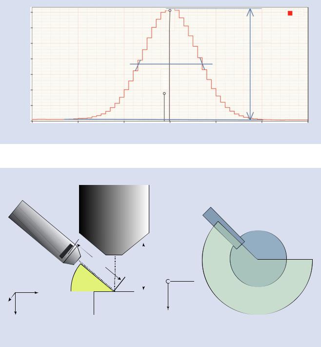
The resolution is a measure of the performance of an EDS detector. Since the resolution depends upon X-ray energy in a predictable manner, the resolution is by long established standard reported as the “full width half maximum” (FWHM) of the Mn Kα peak (5.899 keV).
The full width at half-maximum is defined as the width of a peak as measured half way from the base to the peak. This is illustrated in the . Fig. 17.5. The full height is measured from the level of the continuum background to the top of the peak. A line is drawn across the peak at half the full height. To account for the finite bin width, a line is drawn on each side of the peak from the center of the bin above the line to the center of the bin below the line. The intersection of this diagonal line is assumed to be the true peak edge position. The width is then measured from these intersection points and calibrated relative to the energy scale.
The graphical method for estimating the FWHM is not as accurate as numerical fitting of Gaussian line shapes. The calibration tool uses the numerical method and is the preferred method (. Fig. 17.6).
Azimuthal Angle
The azimuthal angle describes the angular position of the detector rotated around the optic axis. The azimuthal angle is particularly important when modeling samples that are tilted or have complex morphology.
17.1 · Getting Started With NIST DTSA-II |
|
|
|
|
243 |
|
|
17 |
||
|
Mn |
|
|
|
|
|
|
|||
|
|
|
|
|
|
|
||||
|
35 000 |
|
|
|
|
|
Mn 1 |
|||
|
30 000 |
|
|
L3-K |
|
|
|
|
|
|
|
|
|
|
|
|
|
|
|
|
|
|
25 000 |
|
|
|
|
Full height |
|
|
|
|
Counts |
20 000 |
|
|
|
|
|
|
|
|
|
15 000 |
|
|
Mn |
|
|
|
|
|
|
|
|
10 000 |
|
|
L2-K |
|
|
|
|
|
|
|
|
|
|
|
|
|
|
|
|
|
|
5 000 |
|
|
|
|
|
|
|
|
|
|
0 |
|
|
|
|
|
|
|
|
|
|
5 600 |
5 700 |
5 800 |
5 900 |
6 000 |
6 100 |
6 200 |
|||
Energy (eV)
. Fig. 17.5 Estimating the full width at half-maximum peak width. This peak is approximately 139 eV FWHM which you can confirm with a ruler
Side view
Electron column
Detector |
snout |
|
|
DD |
|
|
Elevation |
|
X |
|
|
|
Sample |
|
Y |
|
|
|
|
|
Z |
|
|
|
|
|
WD: Working distance |
|
|
DD: Detector distance |
|
|
Top view looking down
WD
 X
X
Azimuth
Y
. Fig. 17.6 Definitions of elevation angle and azimuthal angle
Gold Layer, Aluminum Layer, Nickel Layer
Detector crystals typically have conductive layers on their front face to ensure conductivity. These layers can be constructed by depositing various different metals on the surface. The absorption profiles of these layers will decrease the efficiency of the detector. The layer thicknesses are particularly relevant for simulation; however, other uncertainties usually exceed the effect of the conductive layer.
Dead Layer
The dead layer is an inactive or partially active layer of silicon on the front face of the detector. The dead layer will absorb some X-rays (particularly low energy X-rays) and produce few to no electron–hole pairs. The result is a fraction of X-rays which produce no signal or a smaller signal than their energy would suggest. The result is twofold: The first effect is a diminishment of the number of low energy X-rays detected. The
\244 Chapter 17 · DTSA-II EDS Software
second effect is a low energy tail, called incomplete charge collection, on low energy X-ray peaks.
The dead layer in modern detectors is very thin and typically produces very little incomplete charge collection. Older Si(Li) detectors had thicker layers and worse incomplete charge collection.
Zero Strobe Discriminator (. Figs. 17.7 and 17.8)
The zero strobe discriminator is an energy below which all spectrum counts will be set to zero before many spectrum processing operations are performed.
The zero strobe is an artificial peak inserted by the detector electronics at 0 eV. The zero strobe is used to automatically determine the noise performance of the detector and to automatically adjust the offset of the detector to compensate for shifts in calibration. The zero strobe does not interfere with real X-ray events because it is located below the energies at which the detector is sensitive.
Some vendors automatically strip out the zero strobe out before presenting the spectrum. Others leave it in because it can provide useful information. When it does appear, it can negatively impact processing low energy peaks. To mitigate this problem, the zero strobe discriminator can be used to strip the zero strobe from the spectrum. The zero strobe dis-
criminator should be set to an energy just above the high energy tail of the zero strobe.
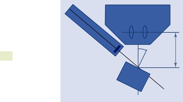
Material Editor Dialog (. Figs. 17.9, 17.10, 17.11, 17.12, 17.13, and 17.14)
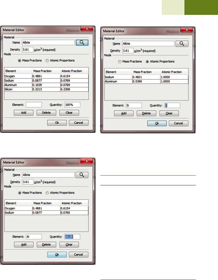
The material editor dialog is used to enter compositional and density information throughout DTSA-II. This dialog allows you to enter compositional information either as mass fractions or atomic fractions. It also provides shortcut mechanisms for looking up definitions in a database or entering compositions using the chemical formula.
Method 1: Mass fractions (see . Fig. 17.10) Method 2: Atomic fractions (see . Fig. 17.11) Method 3: Chemical formula (see . Fig. 17.12) Method 4: Database lookup (see . Fig. 17.13)
Method 5: Advanced chemical formulas (see . Fig. 17.16)
So if your database contains a definition for “Albite” and
you press the search button  , the table will be filled with the mass and atomic fractions and the density as recorded in the database for “Albite.” The database is updated each time you select the “Ok” button. Over time, it is possible to fill the database with every material that you commonly see in your laboratory. The name “unknown” is special and is never saved to the database.
|
600 000 |
|
|
|
Cu |
Counts |
400 000 |
|
|
|
|
|
|
|
|
|
|
|
200 000 |
|
|
|
|
|
0 |
|
|
|
|
|
-500 |
0 |
500 |
1 000 |
1500 |
Energy (eV)
17
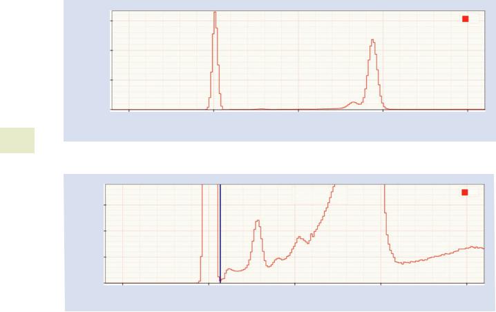
. Fig. 17.7 A raw Cu spectrum showing the zero strobe peak centered at 0 eV and the Cu L peaks centered near 940 eV
Counts
|
68 eV |
Cu |
|
6 000 |
Cu |
||
166 |
|||
|
4 000
2 000
0
-500 |
0 |
500 |
1 000 |
1500 |
|
|
Energy (eV) |
|
|
. Fig. 17.8 The blue line shows an appropriate placement of the zero strobe discriminator between the high energy edge of the zero strobe and the start of the real X-ray data
245 |
17 |
17.2 · Simulation in DTSA-II
. Fig. 17.9 The material editor dialog. Materials are defined by a name (“Albite”), a density (“3.61 g/cm3”), and a mapping between elements and quantities. Albite is defined as NaAlSi3O8 which is equivalent to the mass fractions and atomic fractions displayed in the table
. Fig. 17.11 The relative amount of each element in atomic fractions may be entered manually using the “Element” and “Quantity” edit boxes and the “Add” button. Note that the mode radio button is set to “Atomic Proportions” and that the quantity is entered as a number of atoms in a unit cell. The element may be specified by the common abbreviation (“Si”), the full name (“silicon”) or the atomic number (“14”)
. Fig. 17.10 The relative amount of each element in mass fractions may be entered manually using the “Element” and “Quantity” edit boxes and the “Add” button. Note that the mode radio button is set to “Mass Fractions” and that the quantity is entered in percent but displayed in mass fractions, so “10.29” corresponds to a mass fraction of “0.1029”. The element may be specified by the common abbreviation (“Al”), the full name (“aluminum”) or the atomic number (“13”)
17.2\ Simulation inDTSA-II
17.2.1\ Introduction
Simulation, particularly Monte Carlo simulation, is a powerful tool for understanding the measurement process. Without the ability to visualize how electrons and X-rays interact with the sample, it can be very hard to predict the significance of a measurement. Does the incident beam remain within the sample? Where are the measured X-rays coming from? Can I choose better instrumental conditions for the measurements? Without simulation, these insight can only be gained with years of experience or based on simple rules of thumb.
Too often we are asked to analyze non-ideal samples. Monte Carlo simulation is one of the few mechanisms we have to ground-truth these measurements. Consider the humble particle. When is it acceptable to consider a particle to be essentially bulk and what are the approximate errors associated with this assumption?
17.2.2\ Monte Carlo Simulation
Monte Carlo models are particularly useful because they permit the simulation of arbitrarily complex sample geometries. NIST DTSA-II provides a handful of different
246\ Chapter 17 · DTSA-II EDS Software
. Fig. 17.12 It is possible to enter the chemical formula directly into the “Name” edit box. When the search button is pressed the chemical formula will be parsed and the appropriate mass and atomic fractions entered into the table. Capitalization of the element abbreviations is important as “CO” is very different from “Co”—one is a gas and the other a metal. More complex formulas like fluorapatite (“Ca5(PO4)3F”) can be entered using parenthesis to group terms. It is important that the formula is unambiguous. Once the formula has been parsed you may specify a new operator friendly name for the material like “Albite”of “Fluorapatite” in the “Name” edit box
common geometries through the graphical user interface. More complex geometries can be simulated using the scripting interface.
Monte Carlo modeling is based on simulating the trajectories of thousands of electrons and X-rays. The simulated 17 electrons are given an initial energy and trajectory which models the initial energy and trajectory of electrons from an SEM gun. The simulated electrons scatter and lose energy as their trajectories take them through the sample. Occasionally, an electron may ionize an atom and generate a characteristic X-ray. Occasionally, an electron may decelerate and generate a bremsstrahlung photon. The X-rays can be tracked from the point of generation to a simulated detector. A simulated spectrum can be accumulated. If care is taken modeling the electron transport and the X-ray interactions, the simulated spectrum can mimic a measured spectrum.
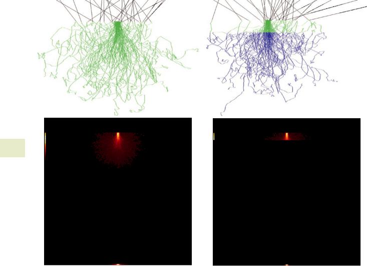
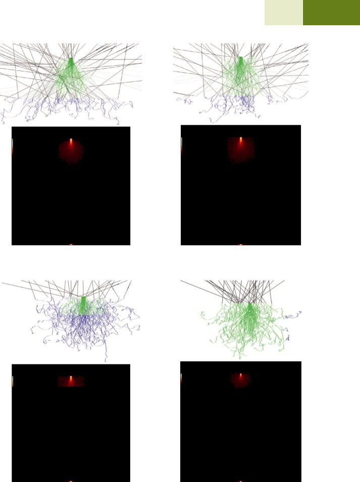
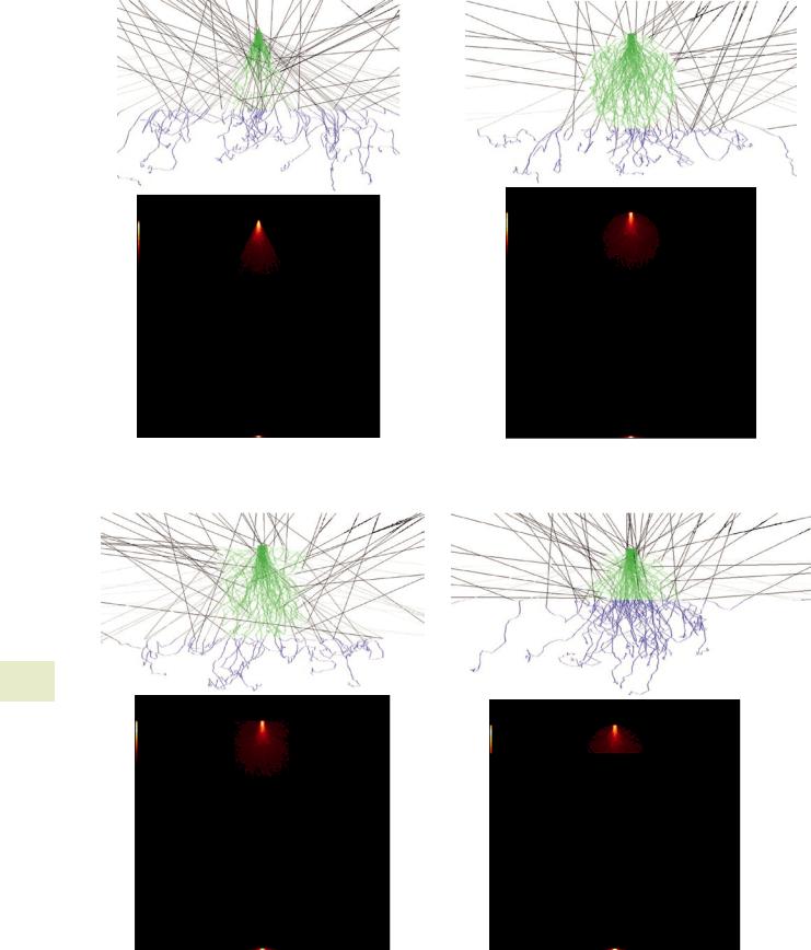
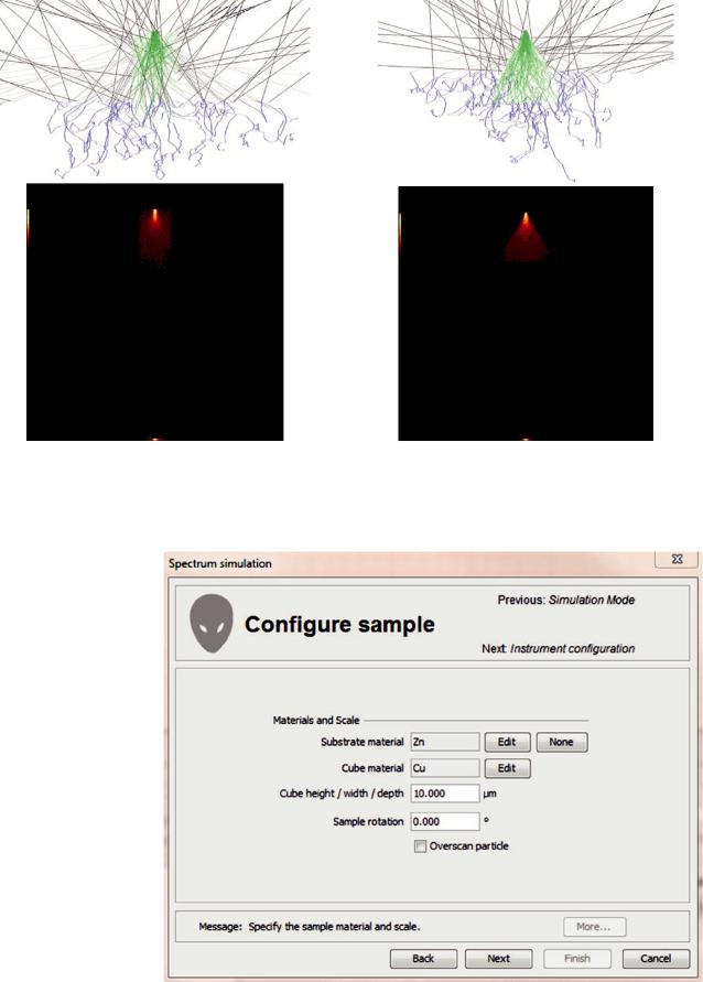
Other data such as emitted intensities, emission images, trajectory images and excitation volumes can be accumulated.
Multi-element materials are modeled as mass-fraction averaged mixtures of elements. Complex sample geometries can be constructed out of discrete sample shapes that include blocks, spheres, cylinders, regions bounded by planar surfaces, and sums and differences of the basic shapes. In this way, it is possible to model arbitrarily complex sample geometries.
. Fig. 17.13 To assist the user, DTSA-II maintains a database of materials. Each time the user enters a new material or redefines an old material, the database is updated. The database is indexed by “Name”
. Fig. 17.14 Albite (“NaAlSi3O8”) and anorthite (“CaAl2Si2O8”) represent end members of the plagioclase solid solution series. To calculate a admixture of 50 % by mass albite and 50 % by mass anorthite, you can enter the formula “0.5*NaAlSi3O8 + 0.5*CaAl2Si2O8”. Other admixtures of stoichiometric compounds can be calculated in a similar manner. Remember to provide a user friendly name for the database
17.2 · Simulation in DTSA-II
17.2.3\ Using theGUI ToPerform a Simulation
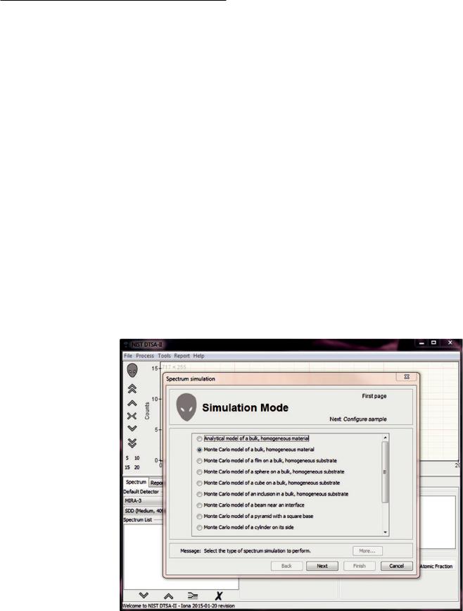
The simplest way to simulate one of an array of common sample geometries in through the “simulation alien.” The “simulation alien” is a dialog that takes you step-by-step through the process of simulating an X-ray spectrum. The dialog requests information that defines the sample geometry, the instrument, and detector, the measurement conditions and the information to simulate. The results of the simulation include a spectrum, raw intensity data, electron trajectory images, X-ray emission images, and excitation volume information. The “simulation alien” is accessed through the “Tools” application menu (. Fig. 17.15).
Many different common sample geometries are available through the “simulation alien.”
55 Analytical model of a bulk, homogeneous material.
55A φ(ρz)-based analytical spectrum simulation model. This model simulates a spectrum in a fraction of a second but is only suited to bulk samples.
55 Monte Carlo model of a bulk, homogeneous material. 55The Monte Carlo equivalent of the φ(ρz)-based
analytical spectrum simulation model (see . Fig. 17.16). 55 Monte Carlo model of a film on a bulk, homogeneous
substrate.
55A model of a user specified thickness film on a substrate (or, optionally, unsupported) (see
. Fig. 17.17).
55 Monte Carlo model of a sphere on a bulk, homogeneous substrate (see . Fig. 17.18).
|
|
247 |
|
|
17 |
|
|
|
|
|
|
|
55A model of a user specified radius sphere on a |
|
|||
|
substrate (or, optionally, unsupported). |
|
|||
55 |
Monte Carlo model of a cube on a bulk, homogeneous |
|
|||
|
substrate. |
|
|||
|
55A model of a user specified size cube on a substrate |
|
|||
|
(or, optionally, unsupported) (see . Fig. 17.19). |
|
|||
55 |
Monte Carlo model of an inclusion on a bulk, homoge- |
|
|||
|
neous substrate. |
|
|||
|
55A model of a block inclusion of specified square cross |
|
|||
|
section and specified thickness in a substrate (or, |
|
|||
|
optionally, unsupported) (see . Fig. 17.20). |
|
|||
55 |
Monte Carlo model of a beam near an interface. |
|
|||
|
55A model of two materials separated by a vertical |
|
|||
|
interface nominally along the y-axis. The beam can be |
|
|||
|
placed a distance from the interface in either material. |
|
|||
|
Positive distances place the beam in the primary |
|
|||
|
material and negative distances are in the secondary |
|
|||
|
material (see . Fig. 17.21). |
|
|||
55 |
Monte Carlo model of a pyramid with a square base. |
|
|||
|
55The user can specify the length of the base edge and |
|
|||
|
the height of the pyramid (see . Fig. 17.22). |
|
|||
55 |
Monte Carlo model of a cylinder on its side |
|
|||
|
55The user can specify the length and diameter of the |
|
|||
|
cylinder (see . Fig. 17.23). |
|
|||
55 |
Monte Carlo model of a cylinder on its end |
|
|||
|
55The user can specify the length and diameter of the |
|
|||
|
cylinder (see . Fig. 17.24). |
|
|||
55 |
Monte Carlo model of a hemispherical cap |
|
|||
|
55The user can specify the radius of the hemispherical cap |
|
|||
|
(see . Fig. 17.25). |
|
|||
. Fig. 17.15 Simulation mode window in DTSA-II
\248 Chapter 17 · DTSA-II EDS Software
55 Monte Carlo model of a block
55The user can specify the block base (square) and the height.
55 Monte Carlo model of an equilateral prism
55The user can specify the edge of the triangle and the length of the prism (. Figs. 17.16, 17.17, 17.18, 17.19,
17.20, 17.21, 17.22, 17.23, 17.24, 17.25, 17.26, 17.27, and 17.28).
Each simulation mode takes different parameters to configure the sample geometry. This page is for the simulation of a cube which requires two materials (substrate and cube), the dimensions of the cube and the sample rotation.
The sample rotation parameter is available for all modes for which are not rotationally invariant. The best way to understand the sample rotation parameter is to imagine rotating the sample about the optic axis at the point on the
sample at which the beam intersects (. Figs. 17.29, 17.30, and 17.31).
All the models require you to specify at least one material. The material editor (described elsewhere) allows you to specify the material. Since the density is a critical parameter, you must specify it (. Fig. 17.32).
Simulations are designed to model the spectra you could collect on your instrument with your detector. By default, the simulation “instrument configuration” page assumes that you want to simulate the “default detector” as specified on the main “Spectrum” tab. However, you can specify a different instrument, detector and calibration if you desire.
You also need to specify an incident beam energy. This is the kinetic energy with which the electrons strike the sample and is specified in kilo-electronvolts (keV).
The probe dose determines the relative intensity in the spectrum. Probe dose is specified in nano-amp seconds
1.44 µm × 1.44 µm |
1.62 µm × 1.62 µm |
Cu K-L3 |
1.81 µm × 1.81 µm |
Zn K-L3 |
2.03 µm × 2.03 µm |
17
1.26E0 |
Emission |
1.06E0 |
Emission |
. Fig. 17.16 Bulk, homogeneous material |
. Fig. 17.17 Thin film on substrate. Parameters: film thickness |
249 |
17 |
17.2 · Simulation in DTSA-II
1.75 µm × 1.75 µm |
1.75 µm × 1.75 µm |
Zn K-L3 |
2.19 µm × 2.19 µm |
Zn K-L3 |
2.19 µm × 2.19 µm |
1.05E0 |
Emission |
1.05E0 |
Emission |
. Fig. 17.18 Spherical particle on a substrate. Parameters: Sphere’s radius
. Fig. 17.19 Cubic particle on a substrate. Parameters: Cube dimension
1.75 µm × 1.75 µm |
3.2 µm × 3.2 µm |
Zn K-L3 |
2.19 µm × 2.19 µm |
Zn K-L3 |
4 µm × 4 µm |
|
|
1.18E0 |
Emission |
3.16E0 |
Emission |
. Fig. 17.20 Block inclusion in substrate. Parameters: Thickness and |
. Fig. 17.21 Interface between two materials. Parameters: Distance |
edge length |
from interface |
\250 Chapter 17 · DTSA-II EDS Software
1.75 µm × 1.75 µm
Zn K-L3 |
2.19 µm × 2.19 µm |
9.13E-1 |
Emission |
. Fig. 17.22 Square pyramid on a substrate. Parameters: Height and base edge length
1.75 µm × 1.75 µm
17
Zn K-L3 |
2.19 µm × 2.19 µm |
1.18E0 |
Emission |
. Fig. 17.24 Cylinder (can) on end on substrate. Parameters: Height and fiber diameter
1.75 µm × 1.75 µm
Zn K-L3 |
2.19 µm × 2.19 µm |
1.15E0 |
Emission |
. Fig. 17.23 Cylinder (fiber) on substrate. Parameters: Fiber diameter and length
1.75 µm × 1.75 µm
Zn K-L3 |
2.19 µm × 2.19 µm |
1.14E0 |
Emission |
. Fig. 17.25 Hemispherical cap on substrate. Parameters: Cap radius
17.2 · Simulation in DTSA-II
1.67 µm × 1.67 µm
Zn K-L3 |
2.09 µm × 2.09 µm |
1.05E0 |
Emission |
. Fig. 17.26 Rectangular block on substrate. Parameters: Block height and base edge length
. Fig. 17.28 “Configure sample” menu
251 |
|
17 |
|
|
|
1.75 µm × 1.75 µm
Zn K-L3 |
2.19 µm × 2.19 µm |
1.08E0 |
Emission |
. Fig. 17.27 Triangular prism on substrate. Parameters: Triangle edge and prism lengths
252\ Chapter 17 · DTSA-II EDS Software
. Fig. 17.29 a Shows how a pyramid with square base model rotates and b shows how a beam near an interface model rotates. Both figures take the perspective of looking down along the optic axis at the sample. The shortest distance to the interface is maintained in . figure b
a
x |
x |
y |
y |
|
|
b |
|
|
x |
|
x |
y |
y |
|
1.75 µm × 1.75 µm |
1.75 µm × 1.75 µm |
1.75 µm × 1.75 µm |
Zn K-L3 |
2.19 µm × 2.19 µm Zn K-L3 |
2.19 µm × 2.19 µm Zn K-L3 |
2.19 µm × 2.19 µm |
17
1.15EO |
Emission 1.17EO |
Emission 1.12EO |
Emission |
Sample rotation: 0 degrees |
Sample rotation: 45 degrees |
Sample rotation: 90 degrees |
|
. Fig. 17.30 A fiber rotated through 0°, 45°, and 90°
253 |
17 |
17.2 · Simulation in DTSA-II
. Fig. 17.31 “Material editor” menu
. Fig. 17.32 “Instrument configuration” menu
\254 Chapter 17 · DTSA-II EDS Software
(nA · s = nC). This quantity is a product of the probe current (nA) and the spectrum acquisition live-time (seconds.) Remember the probe current is a measure of the actual number of electrons striking the sample per unit time, so the probe dose is equivalent to a number of electrons striking the sample during the measurement. Doubling the dose doubles the number of electrons striking the sample and thus also doubles the average number of X-rays generated in the sample.
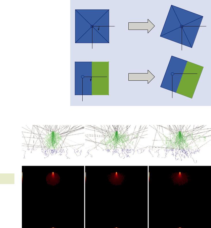
The incidence angle (nominally 0°) allows you to simulate a tilted sample (. Fig. 17.33).
The incident angle is defined relative to the optic axis. The pivot occurs at the surface of the sample, which is placed at the detector’s optimal working distance. A positive rotation is towards the X-axis (an azimuth of 0°) and a negative rotation towards the –X axis (an azimuth of 180°.) The detector displayed is at an azimuth of 180°. A negative incidence angle would tilt the sample toward the detector. Arbitrary tilts may be simulated by moving the detector around the azimuth
(. Figs. 17.33, 17.34, 17.35, and 17.36).
The “other options” page allows you to specify whether the spectrum is simulated with or without variance due to count statistics. If you select to “apply simulated count sta-
tistics,” you may also select to output multiple spectra based on the simulated spectrum but differ by pseudorandom count statistics. You may also select to run additional simulated electron trajectories. The number of simulated electron trajectories determines the simulation to simulation variance in characteristic X-ray intensities. The default number of electron trajectories typically produces about 1 % variance. The variance decreases as the square-root of the number of simulated trajectories. You may also specify which X-ray generation modes to simulate including both characteristic and bremsstrahlung primary emission and secondary emission due to characteristic primary emission or bremsstrahlung primary emission (. Figs. 17.37, 17.38, and 17.39).
The “configure VP” page provides an advanced option to simulate the beam scatter in a variable-pressure or environmental SEM. If the check box is selected, you may select a gas
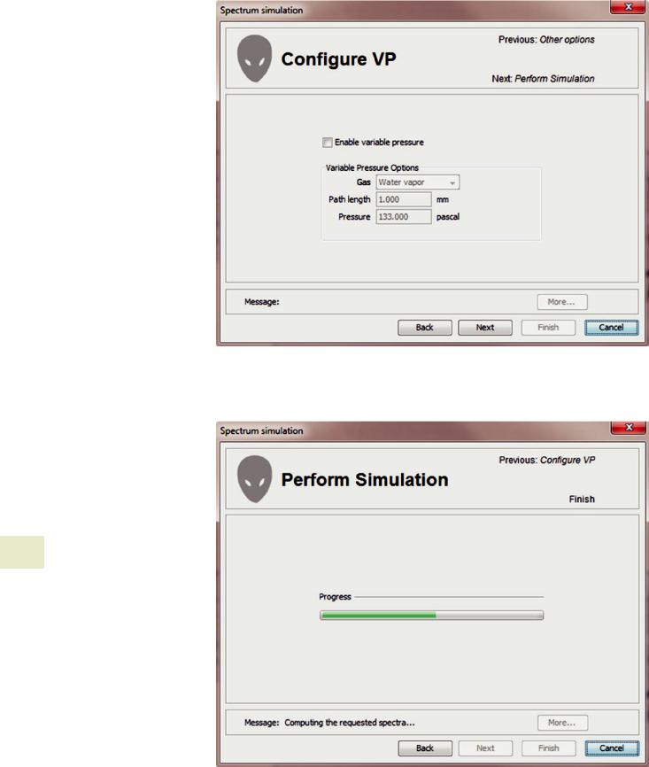
(“water,” “helium,” “nitrogen,” “oxygen” or “argon”), a gas path length and a nominal pressure. The gas path length is the distance from the final pressure limiting aperture to the sample. 1 Torr is equivalent to 133 Pa (. Figs. 17.40 and 17.41).
The primary output of a simulation is a spectrum. The simulated spectrum looks and acts to the best of our ability
. Fig. 17.33 Definition of angles for a tilted specimen
Objective Lens
X |
|
- |
|
ray |
Detector |
|
17 |
Incident |
|
|
|
Angle |
Optimal working Distance
X axis
Sample
axis
17.2 · Simulation in DTSA-II |
|
|
|
255 |
|
|
17 |
|
|
|
|
|
|
|
|
||
|
|
|
|
|
|
|
||
Cu K-L3 |
1.81 µm × 1.81 µm |
Cu K-L3 |
1.81 µm × 1.81 µm |
Cu K-L3 |
1.81 µm × 1.81 µm |
|
||
1.31EO |
Emission |
1.26EO |
Emission |
1.27EO |
Emission |
Sample tilt: -15 degrees |
|
Sample tilt: 0 degrees |
|
Sample tilt: 15 degrees |
|
Cu K-L3 |
1.81 µm × 1.81 µm |
Cu K-L3 |
1.81 µm × 1.81 µm |
Cu K-L3 |
1.81 µm × 1.81 µm |
1.35EO |
Emission |
1.12EO |
Emission |
1.3EO |
Emission |
Sample tilt: 30 degrees |
|
Sample tilt: 45 degrees |
|
Sample tilt: 60 degrees |
|
. Fig. 17.34 Tilting a bulk sample |
|
|
|
|
|
Zn K-L3 |
2.19 µm × 2.19 µm Zn K-L3 |
2.19 µm × 2.19 µm Zn K-L3 |
2.19 µm × 2.19 µm |
1.12EO |
Emission 1.05EO |
Emission 1.07EO |
Emission |
Sample tilt: -30 degrees |
Sample tilt: 0 degrees |
Sample tilt: 30 degrees |
. Fig. 17.35 Tilting a spherical sample |
|
|
256\ Chapter 17 · DTSA-II EDS Software
. Fig. 17.36 Menu for selecting number of trajectories, repetitions, and X-ray generation modes
|
to simulate measured spectra like a spectrum collected from |
|
the specified material under the specified conditions on the |
|
specified detector. You can treat simulated spectra like |
|
measured spectra in the sense that you can simulate an |
|
“unknown” standards and reference spectra and quantify the |
|
“unknown” as though it had been measured (. Fig. 17.42). |
|
The report tab contains additional details about the simu- |
|
lation including configuration and results information. The |
|
first table summarizes the simulation configuration |
|
parameters. This table is available for all simulation modes |
17 |
(. Fig. 17.43). |
The “simulation results” table contains additional details derived from the simulation. The first two lines contain links to the simulated spectrum and a Virtual Reality Markup Language (VRML) representation of the sample and electron trajectories. The subsequent rows contain raw data detailing the generation and emission of various different kinds of characteristic X-rays. Only those modes which were selected will be available. The generated X-rays column tabulates the relative number of X-rays
generated within the sample and emitted into a milli-stera- dian. The emitted column tabulates the X-rays that are generated and also escape the sample in the direction of the detector. The ratio is the fraction of generated X-rays that escape the sample in the direction of the detector. The final rows compare the relative amount of characteristic fluorescence to the amount of primary characteristic and bremsstrahlung emission (. Fig. 17.44).
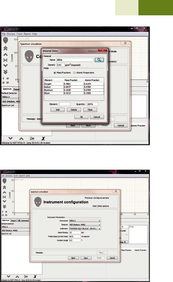
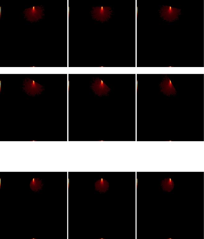
The emission images show where the measured X-rays were generated. Because the images only display X-rays that escape the sample, the distinction between the strongly absorbed X-rays like the O K-L3 (Kα) and the less strongly absorbed like the Si K-L3 (Kα) is evidenced by the flattened emission profile in the Si K-L3 image. The last image shows the first 100 simulated electron trajectories (down to a kinetic energy of 50 eV.) The color of the trajectory segment varies as the electron passes through the different materials present in the sample. The gray lines exiting the top of the image are backscattered electrons (trajectories in vacuum).
17.2 · Simulation in DTSA-II
|
10000 |
|
(Log) |
1000 |
|
|
|
|
Counts |
100 |
|
|
|
|
|
10 |
|
|
1 |
0 |
|
2000 |
|
1500 |
Counts |
1000 |
|
500 |
|
0 |
0
257 |
|
17 |
|
|
|
2 |
4 |
6 |
8 |
10 |
12 |
14 |
|
|
|
Energy (keV) |
|
|
|
2 |
4 |
6 |
8 |
10 |
12 |
14 |
|
|
|
Energy (keV) |
|
|
|
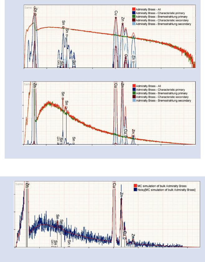
. Fig. 17.37 Simulated admiralty brass (69 % Cu, 30 % Zn, and 1 % Tin) for various different selections of generation modes
Counts
60
40
20
0
0 |
2 |
4 |
6 |
8 |
10 |
12 |
14 |
|
|
|
|
Energy (keV) |
|
|
|
. Fig. 17.38 Simulated admiralty brass (69 % Cu, 30 % Zn, and 1 % Tin) with (blue) and without (red) simulated variation due to count statistics
258\ Chapter 17 · DTSA-II EDS Software
. Fig. 17.39 Menu for selection of variable pressure SEM operating conditions
. Fig. 17.40 The “perform simulation” page shows progress as the electron trajectories are simulated. When the simulation is complete the “finish” button will enable to allow you to close the dialog
17
259 |
17 |
17.2 · Simulation in DTSA-II
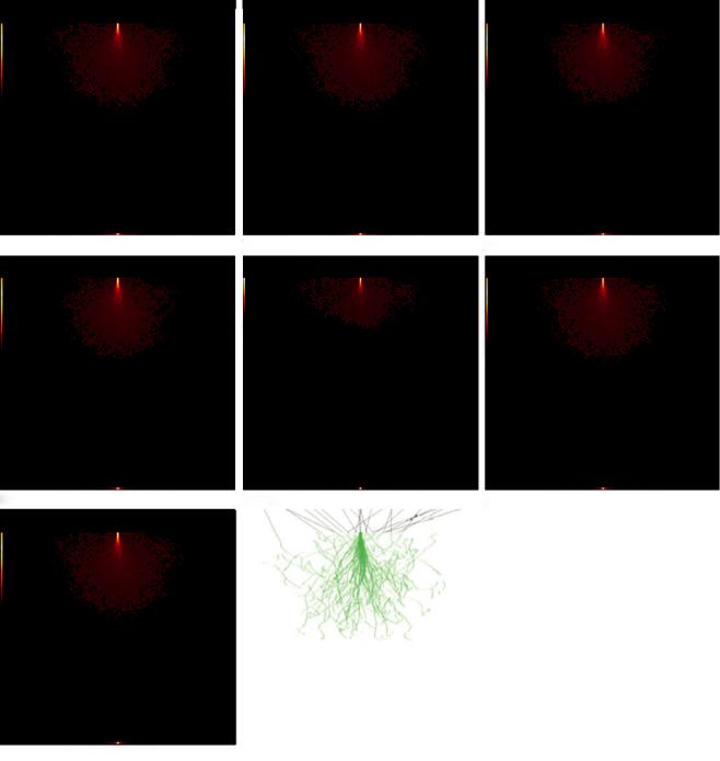
. Fig. 17.41 Simulation results: X-ray spectrum |
|
|
|
|
|
|
||
. Fig. 17.42 Simulation results: |
|
|
|
|
|
|
|
|
|
|
|
|
|
|
|
|
|
configuration record |
|
Simulation Configuration |
|
|
|
|
|
|
|
|
|
|
|
|
|
|
|
|
|
Simulation mode |
Monte Carlo model of a bulk sample |
|
|
|
||
|
|
|
Anorthite |
|
|
|
|
|
|
|
|
Element |
Mass |
Mass Fraction |
Atomic |
|
|
|
|
|
Fraction |
(normalized) |
Fraction |
|
|
|
|
|
|
|
|
|
|||
|
|
|
|
|
|
|
|
|
|
|
Material |
O |
0.4601 |
0.4601 |
0.6154 |
|
|
|
|
|
AI |
0.1940 |
0.1940 |
0.1538 |
|
|
|
|
|
Si |
0.2019 |
0.2019 |
0.1538 |
|
|
|
|
|
Ca |
0.1441 |
0.1441 |
0.0769 |
|
|
|
|
Sample rotation |
0.0° |
|
|
|
|
|
|
|
Sample tilt |
0.0° |
|
|
|
|
|
|
|
Beam energy |
15.0 keV |
|
|
|
|
|
|
|
Probe dose |
60.0 nA.s |
|
|
|
|
|
|
|
Instrument |
MIRA-3 |
|
|
|
|
|
|
|
Detector |
SDD (Medium, 4096) |
|
|
|
|
|
|
|
Calibration |
FWHM[Mn Kα]=130.8 eV - 2014-02-18 00:00 |
|
||||
|
|
Overscan |
False |
|
|
|
|
|
|
|
Vacuum conditions |
High vacuum |
|
|
|
|
|
|
|
Replicas (with poisson noise) |
1 |
|
|
|
|
|
|
|
|
|
|
|
|
|
|

260\ Chapter 17 · DTSA-II EDS Software
. Fig. 17.43 Simulation results: table of X-ray intensities from various sources
17
Simulation Results
Result 1 |
Noisy[MC simulation of bulk Anorthite] #1 |
|
|
||||||||||||
Trajectory view |
VRML World View File |
|
|
|
|
|
|
|
|
||||||
|
|
|
|
|
|
|
|
|
|
|
|
|
|
||
|
Transition |
Generated |
Emitted |
|
|
Ratio |
|||||||||
|
1/msR |
|
|
1/msR |
|
|
|
|
(%) |
||||||
|
|
|
|
|
|
|
|
|
|
||||||
|
O AII |
|
91,816,279.1 |
|
20,029,188.1 |
|
21.8% |
||||||||
|
AI Kα |
|
28,067,811.9 |
|
20,031,447.5 |
|
71.4% |
||||||||
Characteristic |
AI Kβ |
|
114,057.1 |
|
84,361.9 |
|
|
74.0% |
|||||||
|
Si Kα |
|
26,960,986.6 |
|
18,249,064.9 |
|
67.7% |
||||||||
|
Si Kβ |
|
459,584.6 |
|
325,666.6 |
|
|
70.9% |
|||||||
|
Ca Kα |
|
8,067,774.1 |
|
7,482,648.8 |
|
92.7% |
||||||||
|
Ca Kβ |
|
859,214.2 |
|
809,593.5 |
|
|
94.2% |
|||||||
|
Transition |
Generated |
|
Emitted |
|
|
Ratio |
|
|
||||||
|
1/msR |
|
|
1/msR |
|
|
(%) |
|
|
|
|||||
|
|
|
|
|
|
|
|
|
|
|
|||||
Characteristic Fluorescence |
O AII |
|
103,834.0 |
|
13,858.1 |
|
|
13.3% |
|
|
|||||
AI Kα |
|
378,534.1 |
|
191,421.7 |
|
|
50.6% |
|
|
||||||
|
|
|
|
|
|
|
|||||||||
|
Si Kα |
|
94,400.7 |
|
24,117.3 |
|
|
25.5% |
|
|
|||||
|
Si Kβ |
|
1,069.9 |
|
|
298.3 |
|
|
|
27.9% |
|
|
|||
|
Transition |
Generated |
|
Emitted |
|
|
Ratio |
|
|
||||||
|
1/msR |
|
|
1/msR |
|
|
(%) |
|
|
|
|||||
|
|
|
|
|
|
|
|
|
|
|
|||||
|
O AII |
|
52,830.4 |
|
8,065.4 |
|
|
15.3% |
|
|
|||||
Bremsstrahulung Fluorescence |
AI Kα |
|
108,362.6 |
|
44,802.6 |
|
|
41.3% |
|
|
|||||
Si Kα |
|
137,984.3 |
|
47,597.8 |
|
|
34.5% |
|
|
||||||
|
Si Kβ |
|
1,563.9 |
|
|
584.1 |
|
|
|
37.3% |
|
|
|||
|
Ca Kα |
|
190,086.6 |
|
93,453.6 |
|
|
49.2% |
|
|
|||||
|
Ca Kβ |
|
20,244.1 |
|
11,052.8 |
|
|
54.6% |
|
|
|||||
|
|
Transition |
|
Generated |
|
Emitted |
|
|
|||||||
|
|
|
(ratio) |
|
|
(ratio) |
|
|
|||||||
|
|
|
|
|
|
|
|
|
|
||||||
|
|
|
O AII |
|
0.0011 |
|
|
0.0007 |
|
|
|
||||
|
|
|
AI Kα |
|
0.0135 |
|
|
0.0096 |
|
|
|
||||
Comparing Characteristic to |
|
|
AI Kβ |
|
0.0000 |
|
|
0.0000 |
|
|
|
||||
Characteristic Fluorescence |
|
|
|
|
|
|
|
|
|||||||
|
|
Si Kα |
|
0.0035 |
|
|
0.0013 |
|
|
|
|||||
|
|
|
|
|
|
|
|
|
|||||||
|
|
|
Si Kβ |
|
0.0023 |
|
|
0.0009 |
|
|
|
||||
|
|
|
Ca Kα |
|
0.0000 |
|
|
0.0000 |
|
|
|
||||
|
|
|
Ca Kβ |
|
0.0000 |
|
|
0.0000 |
|
|
|
||||
|
|
Transition |
|
Generated |
|
Emitted |
|
|
|||||||
|
|
|
(ratio) |
|
|
(ratio) |
|
|
|||||||
|
|
|
|
|
|
|
|
|
|
||||||
|
|
|
O AII |
|
0.0006 |
|
|
0.00004 |
|
|
|||||
Comparing Characteristic to |
|
|
AI Kα |
|
0.0039 |
|
|
0.00022 |
|
|
|||||
|
|
AI Kβ |
|
0.0000 |
|
|
0.00000 |
|
|
||||||
Bremsstrahulung Fluorescence |
|
|
Si Kα |
|
0.0051 |
|
|
0.00026 |
|
|
|||||
|
|
|
|
|
|
|
|
||||||||
|
|
|
Si Kβ |
|
0.0034 |
|
|
0.00018 |
|
|
|||||
|
|
|
Ca Kα |
|
0.0236 |
|
|
0.0125 |
|
|
|
||||
|
|
|
Ca Kβ |
|
0.0236 |
|
|
0.0137 |
|
|
|
||||
|
|
|
|
|
|
|
|
|
|
|
|
|
|
|
|
17.2 · Simulation in DTSA-II |
|
261 |
|
|
17 |
|
|
|
|
|
|
||
|
|
|
|
|
||
Al K-L3 |
5.14 µm × 5.14 µm Al K-L3 |
5.14 µm × 5.14 µm Cl K-L3 |
5.14 µm × 5.14 µm |
|
||
2.5E0 |
Emission |
1.53E-2 |
Emission |
1.02E0 |
Emission |
Al K-M3 |
|
Al K-M3 |
|
Ca K-L3 |
|
Ca K-M3 |
5.14 µm × 5.14 µm |
O K-L3 |
5.14 µm × 5.14 µm |
Si K-L3 |
5.14 µm × 5.14 µm |
1.09E-1 |
Emission 6.33E0 |
Emission 2.51E0 |
Emission |
Ca K-M3 |
O K-L3 |
Si K-L3 |
|
Si K-M3 |
5.14 µm × 5.14 µm |
4.11 µm × 4.11 µm |
|
4.28E-2 |
Emission |
Si K-M3 |
Trajectories |
. Fig. 17.44 Simulation results: X-ray emission images and trajectories