

- •Preface
- •Imaging Microscopic Features
- •Measuring the Crystal Structure
- •References
- •Contents
- •1.4 Simulating the Effects of Elastic Scattering: Monte Carlo Calculations
- •What Are the Main Features of the Beam Electron Interaction Volume?
- •How Does the Interaction Volume Change with Composition?
- •How Does the Interaction Volume Change with Incident Beam Energy?
- •How Does the Interaction Volume Change with Specimen Tilt?
- •1.5 A Range Equation To Estimate the Size of the Interaction Volume
- •References
- •2: Backscattered Electrons
- •2.1 Origin
- •2.2.1 BSE Response to Specimen Composition (η vs. Atomic Number, Z)
- •SEM Image Contrast with BSE: “Atomic Number Contrast”
- •SEM Image Contrast: “BSE Topographic Contrast—Number Effects”
- •2.2.3 Angular Distribution of Backscattering
- •Beam Incident at an Acute Angle to the Specimen Surface (Specimen Tilt > 0°)
- •SEM Image Contrast: “BSE Topographic Contrast—Trajectory Effects”
- •2.2.4 Spatial Distribution of Backscattering
- •Depth Distribution of Backscattering
- •Radial Distribution of Backscattered Electrons
- •2.3 Summary
- •References
- •3: Secondary Electrons
- •3.1 Origin
- •3.2 Energy Distribution
- •3.3 Escape Depth of Secondary Electrons
- •3.8 Spatial Characteristics of Secondary Electrons
- •References
- •4: X-Rays
- •4.1 Overview
- •4.2 Characteristic X-Rays
- •4.2.1 Origin
- •4.2.2 Fluorescence Yield
- •4.2.3 X-Ray Families
- •4.2.4 X-Ray Nomenclature
- •4.2.6 Characteristic X-Ray Intensity
- •Isolated Atoms
- •X-Ray Production in Thin Foils
- •X-Ray Intensity Emitted from Thick, Solid Specimens
- •4.3 X-Ray Continuum (bremsstrahlung)
- •4.3.1 X-Ray Continuum Intensity
- •4.3.3 Range of X-ray Production
- •4.4 X-Ray Absorption
- •4.5 X-Ray Fluorescence
- •References
- •5.1 Electron Beam Parameters
- •5.2 Electron Optical Parameters
- •5.2.1 Beam Energy
- •Landing Energy
- •5.2.2 Beam Diameter
- •5.2.3 Beam Current
- •5.2.4 Beam Current Density
- •5.2.5 Beam Convergence Angle, α
- •5.2.6 Beam Solid Angle
- •5.2.7 Electron Optical Brightness, β
- •Brightness Equation
- •5.2.8 Focus
- •Astigmatism
- •5.3 SEM Imaging Modes
- •5.3.1 High Depth-of-Field Mode
- •5.3.2 High-Current Mode
- •5.3.3 Resolution Mode
- •5.3.4 Low-Voltage Mode
- •5.4 Electron Detectors
- •5.4.1 Important Properties of BSE and SE for Detector Design and Operation
- •Abundance
- •Angular Distribution
- •Kinetic Energy Response
- •5.4.2 Detector Characteristics
- •Angular Measures for Electron Detectors
- •Elevation (Take-Off) Angle, ψ, and Azimuthal Angle, ζ
- •Solid Angle, Ω
- •Energy Response
- •Bandwidth
- •5.4.3 Common Types of Electron Detectors
- •Backscattered Electrons
- •Passive Detectors
- •Scintillation Detectors
- •Semiconductor BSE Detectors
- •5.4.4 Secondary Electron Detectors
- •Everhart–Thornley Detector
- •Through-the-Lens (TTL) Electron Detectors
- •TTL SE Detector
- •TTL BSE Detector
- •Measuring the DQE: BSE Semiconductor Detector
- •References
- •6: Image Formation
- •6.1 Image Construction by Scanning Action
- •6.2 Magnification
- •6.3 Making Dimensional Measurements With the SEM: How Big Is That Feature?
- •Using a Calibrated Structure in ImageJ-Fiji
- •6.4 Image Defects
- •6.4.1 Projection Distortion (Foreshortening)
- •6.4.2 Image Defocusing (Blurring)
- •6.5 Making Measurements on Surfaces With Arbitrary Topography: Stereomicroscopy
- •6.5.1 Qualitative Stereomicroscopy
- •Fixed beam, Specimen Position Altered
- •Fixed Specimen, Beam Incidence Angle Changed
- •6.5.2 Quantitative Stereomicroscopy
- •Measuring a Simple Vertical Displacement
- •References
- •7: SEM Image Interpretation
- •7.1 Information in SEM Images
- •7.2.2 Calculating Atomic Number Contrast
- •Establishing a Robust Light-Optical Analogy
- •Getting It Wrong: Breaking the Light-Optical Analogy of the Everhart–Thornley (Positive Bias) Detector
- •Deconstructing the SEM/E–T Image of Topography
- •SUM Mode (A + B)
- •DIFFERENCE Mode (A−B)
- •References
- •References
- •9: Image Defects
- •9.1 Charging
- •9.1.1 What Is Specimen Charging?
- •9.1.3 Techniques to Control Charging Artifacts (High Vacuum Instruments)
- •Observing Uncoated Specimens
- •Coating an Insulating Specimen for Charge Dissipation
- •Choosing the Coating for Imaging Morphology
- •9.2 Radiation Damage
- •9.3 Contamination
- •References
- •10: High Resolution Imaging
- •10.2 Instrumentation Considerations
- •10.4.1 SE Range Effects Produce Bright Edges (Isolated Edges)
- •10.4.4 Too Much of a Good Thing: The Bright Edge Effect Hinders Locating the True Position of an Edge for Critical Dimension Metrology
- •10.5.1 Beam Energy Strategies
- •Low Beam Energy Strategy
- •High Beam Energy Strategy
- •Making More SE1: Apply a Thin High-δ Metal Coating
- •Making Fewer BSEs, SE2, and SE3 by Eliminating Bulk Scattering From the Substrate
- •10.6 Factors That Hinder Achieving High Resolution
- •10.6.2 Pathological Specimen Behavior
- •Contamination
- •Instabilities
- •References
- •11: Low Beam Energy SEM
- •11.3 Selecting the Beam Energy to Control the Spatial Sampling of Imaging Signals
- •11.3.1 Low Beam Energy for High Lateral Resolution SEM
- •11.3.2 Low Beam Energy for High Depth Resolution SEM
- •11.3.3 Extremely Low Beam Energy Imaging
- •References
- •12.1.1 Stable Electron Source Operation
- •12.1.2 Maintaining Beam Integrity
- •12.1.4 Minimizing Contamination
- •12.3.1 Control of Specimen Charging
- •12.5 VPSEM Image Resolution
- •References
- •13: ImageJ and Fiji
- •13.1 The ImageJ Universe
- •13.2 Fiji
- •13.3 Plugins
- •13.4 Where to Learn More
- •References
- •14: SEM Imaging Checklist
- •14.1.1 Conducting or Semiconducting Specimens
- •14.1.2 Insulating Specimens
- •14.2 Electron Signals Available
- •14.2.1 Beam Electron Range
- •14.2.2 Backscattered Electrons
- •14.2.3 Secondary Electrons
- •14.3 Selecting the Electron Detector
- •14.3.2 Backscattered Electron Detectors
- •14.3.3 “Through-the-Lens” Detectors
- •14.4 Selecting the Beam Energy for SEM Imaging
- •14.4.4 High Resolution SEM Imaging
- •Strategy 1
- •Strategy 2
- •14.5 Selecting the Beam Current
- •14.5.1 High Resolution Imaging
- •14.5.2 Low Contrast Features Require High Beam Current and/or Long Frame Time to Establish Visibility
- •14.6 Image Presentation
- •14.6.1 “Live” Display Adjustments
- •14.6.2 Post-Collection Processing
- •14.7 Image Interpretation
- •14.7.1 Observer’s Point of View
- •14.7.3 Contrast Encoding
- •14.8.1 VPSEM Advantages
- •14.8.2 VPSEM Disadvantages
- •15: SEM Case Studies
- •15.1 Case Study: How High Is That Feature Relative to Another?
- •15.2 Revealing Shallow Surface Relief
- •16.1.2 Minor Artifacts: The Si-Escape Peak
- •16.1.3 Minor Artifacts: Coincidence Peaks
- •16.1.4 Minor Artifacts: Si Absorption Edge and Si Internal Fluorescence Peak
- •16.2 “Best Practices” for Electron-Excited EDS Operation
- •16.2.1 Operation of the EDS System
- •Choosing the EDS Time Constant (Resolution and Throughput)
- •Choosing the Solid Angle of the EDS
- •Selecting a Beam Current for an Acceptable Level of System Dead-Time
- •16.3.1 Detector Geometry
- •16.3.2 Process Time
- •16.3.3 Optimal Working Distance
- •16.3.4 Detector Orientation
- •16.3.5 Count Rate Linearity
- •16.3.6 Energy Calibration Linearity
- •16.3.7 Other Items
- •16.3.8 Setting Up a Quality Control Program
- •Using the QC Tools Within DTSA-II
- •Creating a QC Project
- •Linearity of Output Count Rate with Live-Time Dose
- •Resolution and Peak Position Stability with Count Rate
- •Solid Angle for Low X-ray Flux
- •Maximizing Throughput at Moderate Resolution
- •References
- •17: DTSA-II EDS Software
- •17.1 Getting Started With NIST DTSA-II
- •17.1.1 Motivation
- •17.1.2 Platform
- •17.1.3 Overview
- •17.1.4 Design
- •Simulation
- •Quantification
- •Experiment Design
- •Modeled Detectors (. Fig. 17.1)
- •Window Type (. Fig. 17.2)
- •The Optimal Working Distance (. Figs. 17.3 and 17.4)
- •Elevation Angle
- •Sample-to-Detector Distance
- •Detector Area
- •Crystal Thickness
- •Number of Channels, Energy Scale, and Zero Offset
- •Resolution at Mn Kα (Approximate)
- •Azimuthal Angle
- •Gold Layer, Aluminum Layer, Nickel Layer
- •Dead Layer
- •Zero Strobe Discriminator (. Figs. 17.7 and 17.8)
- •Material Editor Dialog (. Figs. 17.9, 17.10, 17.11, 17.12, 17.13, and 17.14)
- •17.2.1 Introduction
- •17.2.2 Monte Carlo Simulation
- •17.2.4 Optional Tables
- •References
- •18: Qualitative Elemental Analysis by Energy Dispersive X-Ray Spectrometry
- •18.1 Quality Assurance Issues for Qualitative Analysis: EDS Calibration
- •18.2 Principles of Qualitative EDS Analysis
- •Exciting Characteristic X-Rays
- •Fluorescence Yield
- •X-ray Absorption
- •Si Escape Peak
- •Coincidence Peaks
- •18.3 Performing Manual Qualitative Analysis
- •Beam Energy
- •Choosing the EDS Resolution (Detector Time Constant)
- •Obtaining Adequate Counts
- •18.4.1 Employ the Available Software Tools
- •18.4.3 Lower Photon Energy Region
- •18.4.5 Checking Your Work
- •18.5 A Worked Example of Manual Peak Identification
- •References
- •19.1 What Is a k-ratio?
- •19.3 Sets of k-ratios
- •19.5 The Analytical Total
- •19.6 Normalization
- •19.7.1 Oxygen by Assumed Stoichiometry
- •19.7.3 Element by Difference
- •19.8 Ways of Reporting Composition
- •19.8.1 Mass Fraction
- •19.8.2 Atomic Fraction
- •19.8.3 Stoichiometry
- •19.8.4 Oxide Fractions
- •Example Calculations
- •19.9 The Accuracy of Quantitative Electron-Excited X-ray Microanalysis
- •19.9.1 Standards-Based k-ratio Protocol
- •19.9.2 “Standardless Analysis”
- •19.10 Appendix
- •19.10.1 The Need for Matrix Corrections To Achieve Quantitative Analysis
- •19.10.2 The Physical Origin of Matrix Effects
- •19.10.3 ZAF Factors in Microanalysis
- •X-ray Generation With Depth, φ(ρz)
- •X-ray Absorption Effect, A
- •X-ray Fluorescence, F
- •References
- •20.2 Instrumentation Requirements
- •20.2.1 Choosing the EDS Parameters
- •EDS Spectrum Channel Energy Width and Spectrum Energy Span
- •EDS Time Constant (Resolution and Throughput)
- •EDS Calibration
- •EDS Solid Angle
- •20.2.2 Choosing the Beam Energy, E0
- •20.2.3 Measuring the Beam Current
- •20.2.4 Choosing the Beam Current
- •Optimizing Analysis Strategy
- •20.3.4 Ba-Ti Interference in BaTiSi3O9
- •20.4 The Need for an Iterative Qualitative and Quantitative Analysis Strategy
- •20.4.2 Analysis of a Stainless Steel
- •20.5 Is the Specimen Homogeneous?
- •20.6 Beam-Sensitive Specimens
- •20.6.1 Alkali Element Migration
- •20.6.2 Materials Subject to Mass Loss During Electron Bombardment—the Marshall-Hall Method
- •Thin Section Analysis
- •Bulk Biological and Organic Specimens
- •References
- •21: Trace Analysis by SEM/EDS
- •21.1 Limits of Detection for SEM/EDS Microanalysis
- •21.2.1 Estimating CDL from a Trace or Minor Constituent from Measuring a Known Standard
- •21.2.2 Estimating CDL After Determination of a Minor or Trace Constituent with Severe Peak Interference from a Major Constituent
- •21.3 Measurements of Trace Constituents by Electron-Excited Energy Dispersive X-ray Spectrometry
- •The Inevitable Physics of Remote Excitation Within the Specimen: Secondary Fluorescence Beyond the Electron Interaction Volume
- •Simulation of Long-Range Secondary X-ray Fluorescence
- •NIST DTSA II Simulation: Vertical Interface Between Two Regions of Different Composition in a Flat Bulk Target
- •NIST DTSA II Simulation: Cubic Particle Embedded in a Bulk Matrix
- •21.5 Summary
- •References
- •22.1.2 Low Beam Energy Analysis Range
- •22.2 Advantage of Low Beam Energy X-Ray Microanalysis
- •22.2.1 Improved Spatial Resolution
- •22.3 Challenges and Limitations of Low Beam Energy X-Ray Microanalysis
- •22.3.1 Reduced Access to Elements
- •22.3.3 At Low Beam Energy, Almost Everything Is Found To Be Layered
- •Analysis of Surface Contamination
- •References
- •23: Analysis of Specimens with Special Geometry: Irregular Bulk Objects and Particles
- •23.2.1 No Chemical Etching
- •23.3 Consequences of Attempting Analysis of Bulk Materials With Rough Surfaces
- •23.4.1 The Raw Analytical Total
- •23.4.2 The Shape of the EDS Spectrum
- •23.5 Best Practices for Analysis of Rough Bulk Samples
- •23.6 Particle Analysis
- •Particle Sample Preparation: Bulk Substrate
- •The Importance of Beam Placement
- •Overscanning
- •“Particle Mass Effect”
- •“Particle Absorption Effect”
- •The Analytical Total Reveals the Impact of Particle Effects
- •Does Overscanning Help?
- •23.6.6 Peak-to-Background (P/B) Method
- •Specimen Geometry Severely Affects the k-ratio, but Not the P/B
- •Using the P/B Correspondence
- •23.7 Summary
- •References
- •24: Compositional Mapping
- •24.2 X-Ray Spectrum Imaging
- •24.2.1 Utilizing XSI Datacubes
- •24.2.2 Derived Spectra
- •SUM Spectrum
- •MAXIMUM PIXEL Spectrum
- •24.3 Quantitative Compositional Mapping
- •24.4 Strategy for XSI Elemental Mapping Data Collection
- •24.4.1 Choosing the EDS Dead-Time
- •24.4.2 Choosing the Pixel Density
- •24.4.3 Choosing the Pixel Dwell Time
- •“Flash Mapping”
- •High Count Mapping
- •References
- •25.1 Gas Scattering Effects in the VPSEM
- •25.1.1 Why Doesn’t the EDS Collimator Exclude the Remote Skirt X-Rays?
- •25.2 What Can Be Done To Minimize gas Scattering in VPSEM?
- •25.2.2 Favorable Sample Characteristics
- •Particle Analysis
- •25.2.3 Unfavorable Sample Characteristics
- •References
- •26.1 Instrumentation
- •26.1.2 EDS Detector
- •26.1.3 Probe Current Measurement Device
- •Direct Measurement: Using a Faraday Cup and Picoammeter
- •A Faraday Cup
- •Electrically Isolated Stage
- •Indirect Measurement: Using a Calibration Spectrum
- •26.1.4 Conductive Coating
- •26.2 Sample Preparation
- •26.2.1 Standard Materials
- •26.2.2 Peak Reference Materials
- •26.3 Initial Set-Up
- •26.3.1 Calibrating the EDS Detector
- •Selecting a Pulse Process Time Constant
- •Energy Calibration
- •Quality Control
- •Sample Orientation
- •Detector Position
- •Probe Current
- •26.4 Collecting Data
- •26.4.1 Exploratory Spectrum
- •26.4.2 Experiment Optimization
- •26.4.3 Selecting Standards
- •26.4.4 Reference Spectra
- •26.4.5 Collecting Standards
- •26.4.6 Collecting Peak-Fitting References
- •26.5 Data Analysis
- •26.5.2 Quantification
- •26.6 Quality Check
- •Reference
- •27.2 Case Study: Aluminum Wire Failures in Residential Wiring
- •References
- •28: Cathodoluminescence
- •28.1 Origin
- •28.2 Measuring Cathodoluminescence
- •28.3 Applications of CL
- •28.3.1 Geology
- •Carbonado Diamond
- •Ancient Impact Zircons
- •28.3.2 Materials Science
- •Semiconductors
- •Lead-Acid Battery Plate Reactions
- •28.3.3 Organic Compounds
- •References
- •29.1.1 Single Crystals
- •29.1.2 Polycrystalline Materials
- •29.1.3 Conditions for Detecting Electron Channeling Contrast
- •Specimen Preparation
- •Instrument Conditions
- •29.2.1 Origin of EBSD Patterns
- •29.2.2 Cameras for EBSD Pattern Detection
- •29.2.3 EBSD Spatial Resolution
- •29.2.5 Steps in Typical EBSD Measurements
- •Sample Preparation for EBSD
- •Align Sample in the SEM
- •Check for EBSD Patterns
- •Adjust SEM and Select EBSD Map Parameters
- •Run the Automated Map
- •29.2.6 Display of the Acquired Data
- •29.2.7 Other Map Components
- •29.2.10 Application Example
- •Application of EBSD To Understand Meteorite Formation
- •29.2.11 Summary
- •Specimen Considerations
- •EBSD Detector
- •Selection of Candidate Crystallographic Phases
- •Microscope Operating Conditions and Pattern Optimization
- •Selection of EBSD Acquisition Parameters
- •Collect the Orientation Map
- •References
- •30.1 Introduction
- •30.2 Ion–Solid Interactions
- •30.3 Focused Ion Beam Systems
- •30.5 Preparation of Samples for SEM
- •30.5.1 Cross-Section Preparation
- •30.5.2 FIB Sample Preparation for 3D Techniques and Imaging
- •30.6 Summary
- •References
- •31: Ion Beam Microscopy
- •31.1 What Is So Useful About Ions?
- •31.2 Generating Ion Beams
- •31.3 Signal Generation in the HIM
- •31.5 Patterning with Ion Beams
- •31.7 Chemical Microanalysis with Ion Beams
- •References
- •Appendix
- •A Database of Electron–Solid Interactions
- •A Database of Electron–Solid Interactions
- •Introduction
- •Backscattered Electrons
- •Secondary Yields
- •Stopping Powers
- •X-ray Ionization Cross Sections
- •Conclusions
- •References
- •Index
- •Reference List
- •Index
385 |
23 |
23.3 · Consequences of Attempting Analysis of Bulk Materials With Rough Surfaces
etching is usually required to produce contrast from grains at different crystallographic orientations and from compositionally distinct phases by creating surface relief through differential chemical attack and dissolution or by staining through chemical reactions. Such microscopic physical relief creates unwanted topography similar to mechanically produced scratches that can affect SEM/EDS analysis. Additionally, in some cases chemical etching can actually modify the chemical composition of the surface region, so that it is no longer representative of the bulk of the material.
23.3\ Consequences of Attempting Analysis of Bulk Materials With Rough Surfaces
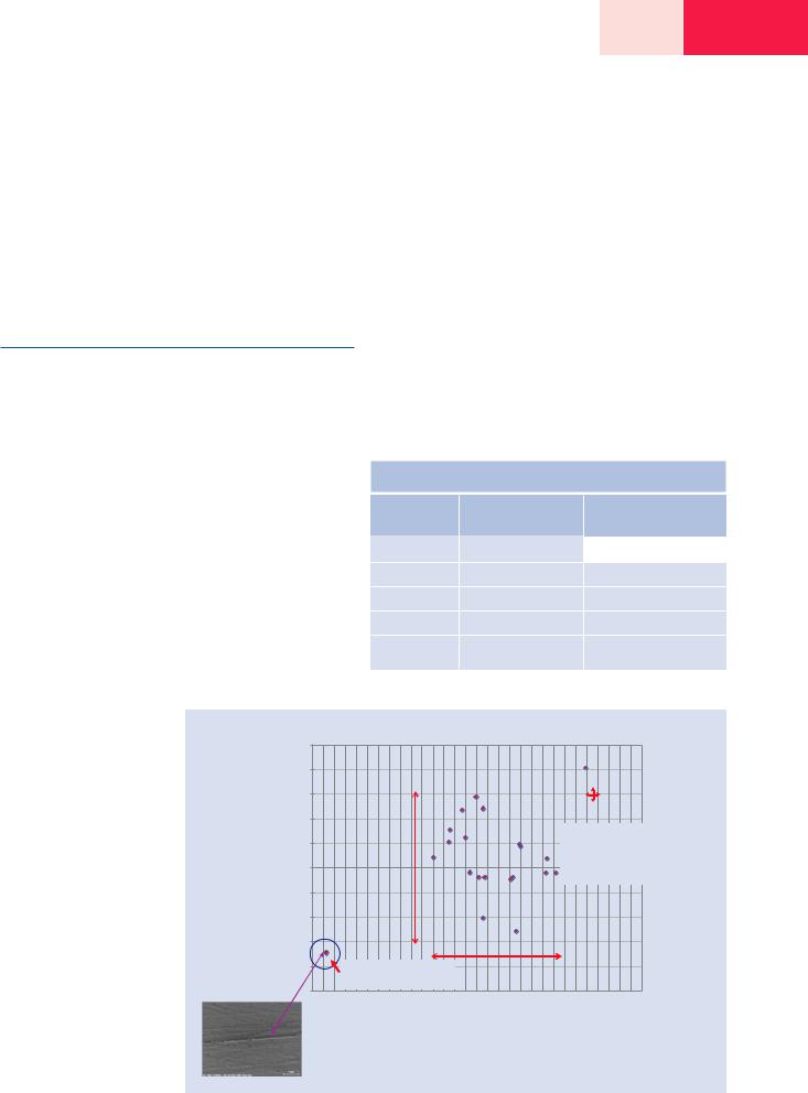
To illustrate the impact of surface topography on microanalysis results, a microscopically homogenous glass (NIST SRM
470 K411) containing several elements (O, Mg, Si, Ca, and Fe) that provide a wide range of range of photon energies, as listed in . Table 23.2, was analyzed with a range of surface topography (Newbury and Ritchie 2013b). Analysis was performed with NIST DTSA-II at E0 = 20 keV using elemental (Mg, Si, Fe) and multi-element (SRM 470 glass K412 for Ca) standards, with oxygen calculated by assumed stoichiometry, followed by normalization of the raw result. When analyzed in the ideal, highly polished (100-nm alumina final polish) flat form, the analyzed concentrations for the Mg and Fe constituents, selected because of their wide difference in photon energies, measured at 20 randomly selected locations show the distribution of results plotted in . Fig. 23.6. The mean of the 20 analyses falls within +1.8 % relative for Fe and −1.0 % relative for Mg (SRM certificate values). Of the 20 analyzed locations, 19 fall within a symmetric cluster that spans
approximately 1% relative along the Mg and Fe concentration axes, while the results for one location fall significantly outside this cluster. This anomalous value was found to be associated with a shallow scratch that remained on the polished surface (location noted on the inset SEM image).
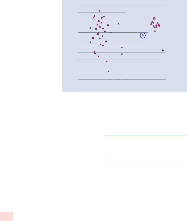
When this highly polished surface was degraded by directional grinding with 1-μm diamond grit, 20 analyses at randomly selected locations produce a much wider scatter in the normalized Mg and Fe concentrations, as shown in . Fig. 23.7, a direct consequence of the effect of surface geometry.
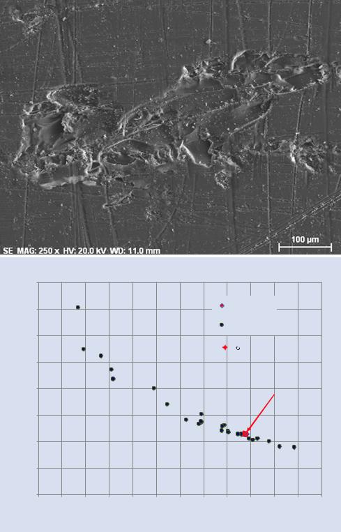
Creating an even more severe topographic feature by gouging the polished surface of K411 with a diamond scribe created the crater seen in the SEM(ET+) SE + BSE image shown in . Fig. 23.8a. Many locations in this gouge crater were analyzed, and the results are plotted in . Fig. 23.8b, showing a very wide range of Mg-Fe results. For comparison, note that the 20 Mg-Fe results from the highly polished surface, including the outlier seen In . Fig. 23.6, are contained within the small red box noted on the plot in . Fig. 23.8b.
. Table 23.2 NIST SRM 470 (Glass K411)
Element |
Mass concentration |
Characteristic X-ray |
|
|
energy (keV) |
|
|
|
O |
0.4236 |
0.523 |
|
|
|
Mg |
0.0885 |
1.254 |
Si |
0.2538 |
1.740 |
Ca |
0.1106 |
3.690 |
Fe |
0.1121 |
6.400 |
. Fig. 23.6 Analysis of polished (0.1-μm alumina final polish) NIST SRM 470 (K411 glass) at E0 = 20 keV with NIST DTSA-II
and standards: elemental (Mg, Si, Fe) and multi-element (SRM 470 K412 glass for Ca), with oxygen calculated by assumed stoichiometry. Normalized results. Note cluster of results and one outlier
11.5 |
Analysis of K411: Bulk polished |
|
|
||
|
|
|
|
|
|
|
|
|
|
BULK |
|
|
|
|
|
1s |
|
|
|
|
|
Mean compared to |
|
|
|
* Av |
|
SRM values |
|
11.4 |
|
|
Fe 11.41 (11.21%) +1.8% rel |
||
|
|
|
|||
(normalizedpercent)weight |
relative1% |
|
|
Mg 8.76 (8.85 %) -1.0% rel |
|
|
|
|
|
||
Fe |
|
|
|
|
|
Outlier possibly a |
|
|
|
|
|
surface finish artifact |
1% relative |
|
|
||
8.65 |
8.7 |
8.75 |
8.8 |
8.85 |
8.9 |
Mg (normalized weight percent)
386\ Chapter 23 · Analysis of Specimens with Special Geometry: Irregular Bulk Objects and Particles
. Fig. 23.7 Analysis of SRM470 (K411 glass) with surface roughness produced by abrading with 1-μm diamond grit
|
11.55 |
1 mm diamond |
|
|
|
|
|
|
|
|
||
|
|
|
|
|
0.1 mm alumina polish |
|
||||||
|
11.5 |
|
|
|
|
|
|
|
||||
|
|
|
|
|
|
|
|
|
|
|
|
|
|
11.45 |
|
|
|
|
|
|
|
|
|
|
|
|
11.4 |
|
|
|
|
|
|
|
|
|
|
|
percent) |
11.35 |
|
|
|
|
|
|
|
|
Mean compared to |
||
|
|
|
|
|
|
|
|
|
||||
11.3 |
|
|
|
|
|
|
|
|
SRM values |
|
||
|
|
|
|
|
|
|
|
Fe 11.41 (11.21%) +1.8% rel |
||||
|
|
|
|
|
|
|
|
|
||||
Fe (weight |
|
|
|
|
|
|
|
|
|
|||
11.25 |
|
|
|
|
|
|
|
|
Mg 8.76 (8.85 %) -1.0% rel |
|||
|
|
|
|
|
K411_Highly polished |
|
|
|||||
|
|
|
|
|
|
|
|
|||||
11.2 |
|
|
|
|
|
K411_1-mu_Diamond |
|
|
||||
|
|
|
|
|
|
|
SRM |
|
||||
|
11.15 |
|
|
|
|
|
|
|
|
|
|
|
|
|
|
|
|
|
|
|
|
|
Certificate |
||
|
11.1 |
|
|
|
|
|
|
|
|
|
values |
|
|
|
|
|
|
|
|
|
|
|
|
|
|
|
11.05 |
|
|
|
|
|
|
|
|
|
|
|
|
11 |
|
|
|
|
|
|
|
|
|
|
|
|
7.8 |
7.9 |
8 |
8.1 |
8.2 |
8.3 |
8.4 |
8.5 |
8.6 |
8.7 |
8.8 |
8.9 |
Mg (weight percent)
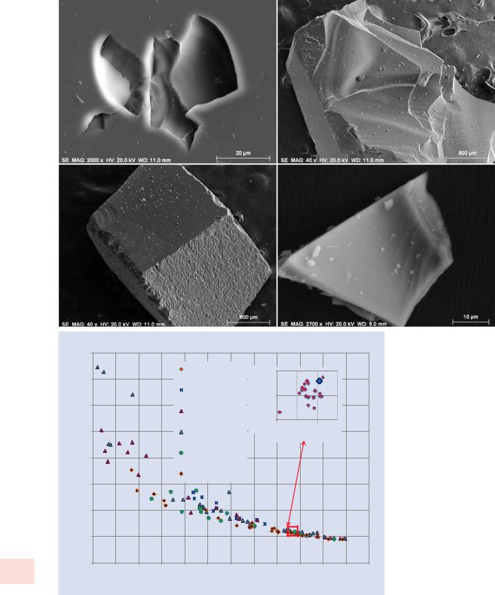
. Figure 23.9a shows examples of additional geometric shapes created with K411 glass: deep, narrow pits from diamond scribe impacts, microscopic particles (major dimensions < 100 μm), and macroscopic particles (major dimensions > 500 μm). When random locations are analyzed on these targets, the range of measured Mg and Fe concentration values is shown in . Fig. 23.9b, covering an order of magnitude in both constituents. This huge range occurs with EDS spectra that were readily measurable despite the severe departure from the ideal flat specimen geometry.
These results demonstrate that the SEM microanalyst must realize that just because an EDS spectrum can be obtained when the stationary beam is placed on a topographic feature of interest, the resulting analysis may be subject to such egregious errors so as to be of little use. Sometimes analysis locations that are surprisingly close on a microscopic scale can produce very different results.
. Figure 23.10 shows a fractured fragment of pyrite (stoichiometric FeS2) which has been analyzed at various locations (conditions: E0 = 20 keV; DTSA-II calculations with Fe and CuS as standards, followed by normalization). Despite the proximity of the analyzed locations, the results vary greatly. Thus, analysis at location 3 produces a nearly perfect match to the stoichiometric values with relative deviation from expected value (RDEV) within ±0.15 %, while analysis at nearby location 9 (about 25 μm away) suffers relative accuracy of ±36 %, while at location 7 (about 50 μm away)
23 the RDEV is ±100 %.
kThe Takeaway
Just because a feature can be observed in an SEM image and an EDS spectrum can be recorded does not mean that a successful and useful quantitative analysis can be performed!
23.4\ Useful Indicators of Geometric Factors
Impact on Analysis
There are strong diagnostic indicators that reveal the impact of geometric factors on analysis:
23.4.1\ The Raw Analytical Total
The raw analytical total is the sum of all the constituents measured (including any constituents such as oxygen calculated on the basis of assumed stoichiometry of the cations). For an ideal flat sample measured with the beam energy selected in the “conventional range” (E0 = 10 keV to 25 keV) and following a standards-based–matrix correction factor protocol, the analytical total typically will fall between 0.98 and 1.02 mass fraction (98–102 wt %), a consequence of the uncertainties inherent in the measurement process (counting statistics) and in the calculated matrix correction factors. If the raw analytical total exceeds this range, it is usually an indication of a deviation in the measurement conditions
(e.g., beam current drift). If the raw analytical total is below this range, this may again indicate a deviation in the
23.4 · Useful Indicators of Geometric Factors Impact on Analysis
. Fig. 23.8 a SEM (ET+) |
|
SE + BSE image of a crater pro- |
|
duced in polished K411 glass |
a |
after gouging with a diamond |
|
scribe. b Plot of the normalized |
|
Mg and Fe concentrations calcu- |
|
lated for measurements at vari- |
|
ous locations in this crater |
|
b
387 |
|
23 |
|
|
|
Analysis with a compromised sample shape: surface gouge crater left by tool impact
Analysis of K411: Bulk polished and tool gouge crater
|
40 |
|
|
|
|
|
|
|
|
|
|
|
|
|
35 |
|
|
|
|
|
|
|
BULK-K411 |
|
|
|
|
|
|
|
|
|
|
|
|
|
|
|
|
|
|
|
|
|
|
|
|
|
|
|
BULK-600grit |
|
|
|
|
percent) |
30 |
|
|
|
|
|
|
|
|
|
|
|
|
|
|
|
|
|
|
|
|
|
1 |
|
|
|
|
25 |
|
|
|
|
|
|
|
|
|
|
|
|
|
|
|
|
|
|
|
|
|
|
|
|
|
|
|
weight |
20 |
|
|
|
|
|
|
|
|
|
|
Extent of ideal |
|
|
|
|
|
|
|
|
|
|
|
flat specimen |
|||
Fe (normalized |
|
|
|
|
|
|
|
|
|
|
|
||
|
|
|
|
|
|
|
|
|
|
|
measurements |
||
15 |
|
|
|
|
|
|
|
|
|
|
|
|
|
10 |
|
|
|
|
|
|
|
|
|
|
|
|
|
|
|
|
|
|
|
|
|
|
|
|
|
|
|
|
5 |
|
|
|
|
|
|
|
|
|
|
|
|
|
0 |
|
|
|
|
|
|
|
|
|
|
|
|
|
0 |
1 |
2 |
3 |
4 |
5 |
6 |
7 |
8 |
9 |
10 |
11 |
12 |
|
|
|
|
|
Mg (normalized weight percent) |
|
|
|
|
||||
\388 Chapter 23 · Analysis of Specimens with Special Geometry: Irregular Bulk Objects and Particles
Analysis with a compromised sample shape
a
b |
Analysis of K411: Bulk polished, 600 Grit, In-hole, Chips, Shards |
|
|
80 |
|
|
|
|
|
|
|
|
|
|
|
|
|
|
70 |
|
|
|
Bulk K411 |
|
weight |
|
11.5 |
Ideal flat surfaceBULK |
|
|
||
|
|
|
|
|
|
|
|
|
|
|
||||
|
|
|
|
|
Shards_overscan |
percent) |
|
|
|
|
|
|||
|
|
|
|
|
Fe (normalized |
11.4 |
|
|
|
|
||||
|
|
|
|
|
|
|
|
|
|
|
|
|||
percent) |
60 |
|
|
|
Shards_fixed-beam |
|
|
|
|
|
||||
|
|
|
|
|
|
|
|
|
||||||
|
|
|
|
|
|
|
11.3 |
|
|
|
|
|||
50 |
|
|
|
Macroscopic chips |
8.6 |
|
8.8 |
|
|
|||||
|
|
|
Mg (normalized weight |
|
|
|||||||||
weight |
|
|
|
|
|
|
|
|
|
|
percent) |
|
|
|
40 |
|
|
|
Surface voids |
|
|
|
|
|
|
|
|
||
|
|
|
|
|
|
|
|
|
|
|
|
|
||
Fe (normalized |
|
|
|
|
|
|
|
|
|
|
|
|
|
|
|
|
|
|
Bulk-600grit |
|
|
|
|
|
|
|
|
||
30 |
|
|
|
|
|
|
|
|
|
|
|
|
|
|
20 |
|
|
|
|
|
|
|
|
|
|
|
|
|
|
|
|
|
|
|
|
|
|
|
|
|
|
|
|
|
|
10 |
|
|
|
|
|
|
|
|
|
|
|
|
|
23 |
0 |
|
|
|
|
|
|
|
|
|
|
|
|
|
0 |
1 |
2 |
3 |
4 |
5 |
6 |
7 |
|
8 |
9 |
10 |
11 |
12 |
|
|
|
|
|
Mg (normalized weight percent) |
|
|
|
|
||||||
|
|
|
|
|
|
|
|
|
||||||
. Fig. 23.9 a Examples of deep narrow pits produced in K411 glass by impacts of a diamond scribe; microscopic particles (major dimensions <50 μm); and macroscopic particles (major dimensions >500 μm).
b Plot of the normalized Mg and Fe concentrations calculated for measurements at various locations on these objects combined with the measurements previously plotted