Добавил:
Опубликованный материал нарушает ваши авторские права? Сообщите нам.
Вуз: Предмет: Файл:
Joseph I. Goldstein, Dale E. Newbury [et al.]. Scanning Electron Microscopy and X-Ray Microanalysis. (2017). (ISBN 978-1-4939-6674-5). (ISBN 978-1-4939-6676-9). (DOI 10.1007978-1-4939-6676-9).pdf
Скачиваний:
20
Добавлен:
11.04.2023
Размер:
68.34 Mб
Скачать

\142 Chapter 9 · Image Defects

coefficient will increase the relative abundance of the high resolution SE1 signal, especially if the specimen consists of much lower atomic number materials, such as biological material. By using the thinnest possible coating, there is only a vanishingly small contribution to electron backscattering which would tend to degrade high resolution performance.

Although gold has a high SE coefficient, pure gold tends to form discontinuous islands whose structure can interfere with visualizing the desired specimen fine scale topographic structure. This island formation can be avoided by using alloys such as gold-palladium, or other pure metals, for example, chromium, platinum, or iridium, which can be deposited by plasma ion sputtering or ion beam sputtering. The elevated pressure in the plasma coater tends to randomize the paths followed by the sputtered atoms, reducing the directionality of the deposition and coating many re-entrant surfaces. For specimens which are thermally fragile, low deposition rates combined with specimen cooling can reduce the damage.

Collapsed area

E-T(+)

40 mm

SE MAG: 500 x HV: 20.0 kV WD: 11.0 mm Px: 0.22 mm

. Fig. 9.13  SEM Everhart–Thornley (positive bias) image of doublesticky conducting tab

9

9.2\ Radiation Damage

Certain materials are susceptible to radiation damage (“beam damage”) under energetic electron bombardment. “Soft” materials such as organic compounds are especially vulnerable to radiation damage, but damage can also be observed in “hard” materials such as minerals and ceramics, especially if water is present in the crystal structure, as is the case for hydrated minerals. Radiation damage can occur at all length scales, from macroscopic to nanoscale. Radiation damage may manifest itself as material decomposition in which mass is actually lost as a volatile gas, or the material may change density, either collapsing or swelling. On an atomic scale, atoms may be dislodged creating vacancies or interstitial atoms in the host lattice.

An example of radiation damage on a coarse scale is illustrated in .Fig. 9.13, which shows a conductive doublesided sticky polymer tab of the type that is often used as a substrate for dispersing particles. This material was found to be extremely sensitive to electron bombardment. As the magnification was successively reduced in a series of 20-s scans, radiation damage in the form of collapse of the structure at the previous higher magnification scan was readily apparent after a single 20-s scan (20 keV and 10 nA). Note that when this tab is used as a direct support for particles, the susceptibility of the tab material to distortion due radiation damage can lead to unacceptable image drift. Instability in the position of the target particle occurs due to changes in the support tape immediately adjacent to the particle of interest where electrons strike, directly at the edges of the image raster and as a result of backscattering off the particle. Other support materials are less susceptible to radiation damage. .Figure 9.14 shows a detail on a different conductive sticky tape material. After a much higher

a

-T(+) E

100 mm

SE MAG: 200 x HV: 20.0 kV WD: 11.0 mm Px: 0.55 mm

b

Collapsed area

100 mm

SE MAG: 200 x HV: 20.0 kV WD: 11.0 mm Px: 0.55 mm

. Fig. 9.14  Conducting tape: a Initial image. b Image after a dose of 15 min exposure at higher magnification (20 keV and 10 nA); Everhart– Thornley (positive bias)

9.3 · Contamination


143


9


dose (15 min of bombardment at 20 keV and 10 nA), a

bombardment. Contamination is a manifestation of radia-


much less significant collapse crater is seen to have formed.

tion damage in which the material that undergoes radiation


It is prudent to examine the behavior of the support materi-

damage is unintentionally present, usually as a result of the


als under electron bombardment prior to use in a particle

original environment of the specimen or as a result of inad-


preparation.

equate cleaning during preparation. Contamination typically


If radiation damage occurs and interferes with successful

arises from hydrocarbons that have been previously depos-


imaging of the structures of interest, the microscopist has

ited on the specimen surface, usually inadvertently. Such


several possible strategies:

compounds are very vulnerable to radiation damage.


\1.\

Follow a minimum dose microscopy strategy.

Hydrocarbons may “crack” under electron irradiation into


\a. \ Radiation damage scales with dose. Use the lowest

gaseous components, leaving behind a deposit of elemental


possible beam current and frame time consistent

carbon. While the beam can interact with hydrocarbons


with establishing the visibility of the features of

present in the area being scanned, electron beam induced


interest. It may be necessary to determine these

migration of hydrocarbons across the surface to actually


parameters for establishing visibility for the particu-

increase the local contamination has been observed (Hren


lar specimen by operating initially on a portion of

1986). Sources of contamination can occur in the SEM itself.


the specimen that can be sacrificed.

However, for a modern SEM that has been well maintained


\b. \ Once optimum beam current and frame time have

and for which scrupulous attention has been paid to degreas-


been established, the SEM can be focused and stig-

ing and subsequently cleanly handling all specimens and


mated on an area adjacent to the features of interest,

stage components, contamination from the instrument itself


and the stage then translated to bring the area of

should be negligible. Ideally, an instrument should be


interest into position. After the image is recorded

equipped with a vacuum airlock to minimize the exposure of


using the shortest possible frame time consistent

the specimen chamber to laboratory air and possible con-


with establishing visibility, the beam should be

tamination during sample exchange. A plasma cleaner that


blanked (ideally into a Faraday cup) to stop further

operates in the specimen airlock during the pump down


electron bombardment while the stored image is

cycle can greatly reduce specimen-related contamination by


examined before proceeding.

decomposing the hydrocarbons, provided the specimen itself


\2.\

Change the beam energy

is not damaged by the active oxygen plasma that is produced.


\

Intuitively, it would seem logical to lower the beam

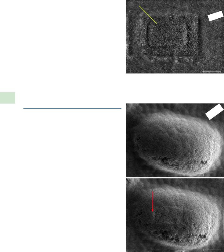
A typical observation of contamination is illustrated in


energy to reduce radiation damage, and depending on

.Fig. 9.15a, where the SEM was first used to image an area at


the particular material and the exact mechanism of

certain magnification and the magnification was subsequently


radiation damage, a lower beam energy may be useful.

reduced to scan a larger area. A “scan rectangle” is observed in


However, the energy deposited per unit volume actually

the lower magnification image that corresponds to the area


increases significantly as the beam energy is lowered!

previously scanned at higher magnification. Within this scan


From the Kanaya–Okayama range, the beam linear

rectangle, the SE coefficient has changed because of the depo-


beam penetration scales approximately as E01.67 so that

sition of a foreign material during electron bombardment,


the volume excited by the beam scales as (RK-O)3 or E05.

most likely a carbon-rich material which has a lower SE coef-


The energy deposited per unit volume scales as E0/E05 or

ficient. Note that the contamination is most pronounced at


1/E04. Thus, the volume density of energy deposition

the edge of the scanned field, where the beam is briefly held


increases by a factor of 104 as the beam energy decreases

stationary before starting the next scanned line so that the


from E0 = 10 keV to E0 = 1 keV. Raising the beam energy

greatest electron dose is applied along this edge.


may actually be a better choice to minimize radiation

“Etching,” the opposite of contamination, can also occur


damage.

(Hren 1986). An example is shown in .Fig. 9.15b, where a


\3.\

Lower the specimen temperature

bright scan rectangle is observed in an image of an aluminum


\Radiation damage mechanisms may be thermally sensistub after reducing the magnification following scanning for

tive. If a cold stage capable of achieving liquid nitrogen

several minutes at higher magnification. In this case, the

temperature or lower is available, radiation damage may

radiation damage has actually removed an overlayer of con-

be suppressed, especially if low temperature operation is

tamination on the specimen, revealing the underlying alumi-

combined with a minimum dose microscopy strategy.

num with its native oxide surface layer (~4 nm thick), which


has an increased SE coefficient compared to the carbon-rich


Contamination

contamination layer.

9.3\

Contamination is usually dose-dependent, so that the high


dose necessary for high resolution microscopy, for example,

“Contamination” broadly refers to a class of phenomena

a small scanned area (i.e., high magnification) with a high

observed in SEM images in which a foreign material is depos-

current density beam from a field emission gun, is likely to

ited

on the specimen as a result of the electron beam

encounter contamination effects. This situation is illustrated

\144 Chapter 9 · Image Defects

a

b

Cu

E0 = 10 keV

. Fig. 9.15a Contamination area observed after a higher magnification scan; Everhart–Thornley (positive bias). The extent of the contamination is visible upon lowering the magnification of the scan, thus

9

increasing the scanned area. b Etching of a surface contamination layer observed during imaging of an aluminum stub; Everhart–Thornley (positive bias); 10 keV and 10 nA

. Fig. 9.16  Contamination observed during dimensional measurements performed under high resolution conditions on a patterned silicon substrate (Postek and Vladar 2014). Note broadening of the structure (right) due to contamination

in .Fig. 9.16, which shows contamination in scanned areas on a patterned silicon sample used for dimensional metrology (Postek and Vladar 2014). The contamination­ in this case was so severe that it actually altered the apparent width of the measured features. To perform successful measurements, the authors developed an aggressive cleaning procedure that minimized contamination effects for this class of specimens. Their strategy may prove useful for other materials as well (Postek and Vladar 2014).

9.4\ Moiré Effects: Imaging What Isn’t

Actually There

An SEM image appears to be continuous, but it is constructed as a regular repeating two-dimensional pattern of pixels. Thus, the viewer is effectively looking at the specimen through a two-dimensional periodic grid, and if the specimen itself has a structure that has a regularly repeating pattern, then a moiré pattern of fringes can form between

145

9

9.4 · Moiré Effects: Imaging What Isn’t Actually There

. Fig. 9.17  Moiré fringe effects observed for the periodic structures in NIST RM 8820 (magnification calibration artifact). Note the different moiré patterns in the different calibration regions; Everhart–Thornley (positive bias) detector

the two patterns. The form of the moiré interference fringes depends on the spacing and orientation of the specimen periodic pattern and the scan pattern. Moiré patterns are maximized when the spatial frequencies of the two patterns are similar or an integer multiple of each other (i.e., they are commensurate). The formation of moiré patterns is illustrated in .Fig. 9.17, which shows various etched patterns in the NIST RM 8820 magnification calibration artifact. The structures have different spacings in each of the fields viewed at the lowest magnification so that different moiré patterns are observed in each field. As the magnification is increased the scan field decreases in size so that the SEM pattern changes its periodicity (spatial frequency), causing

the moiré pattern to change. Finally, at sufficiently high magnification, the specimen periodic structure becomes sufficiently different from the scan pattern that the moiré fringes are lost.

Moiré effects can be very subtle. The periodic bright flares at fine edges, as seen in .Fig. 9.18, are moiré patterns created when the fine scale structure approaches the periodicity of the scan grid.

To avoid interpreting moiré effects as real structures, the relative position and/or rotation of the specimen and the scan grid should be changed. A real structure will be preserved by such an action, while the moiré pattern will change.