

- •Preface
- •Imaging Microscopic Features
- •Measuring the Crystal Structure
- •References
- •Contents
- •1.4 Simulating the Effects of Elastic Scattering: Monte Carlo Calculations
- •What Are the Main Features of the Beam Electron Interaction Volume?
- •How Does the Interaction Volume Change with Composition?
- •How Does the Interaction Volume Change with Incident Beam Energy?
- •How Does the Interaction Volume Change with Specimen Tilt?
- •1.5 A Range Equation To Estimate the Size of the Interaction Volume
- •References
- •2: Backscattered Electrons
- •2.1 Origin
- •2.2.1 BSE Response to Specimen Composition (η vs. Atomic Number, Z)
- •SEM Image Contrast with BSE: “Atomic Number Contrast”
- •SEM Image Contrast: “BSE Topographic Contrast—Number Effects”
- •2.2.3 Angular Distribution of Backscattering
- •Beam Incident at an Acute Angle to the Specimen Surface (Specimen Tilt > 0°)
- •SEM Image Contrast: “BSE Topographic Contrast—Trajectory Effects”
- •2.2.4 Spatial Distribution of Backscattering
- •Depth Distribution of Backscattering
- •Radial Distribution of Backscattered Electrons
- •2.3 Summary
- •References
- •3: Secondary Electrons
- •3.1 Origin
- •3.2 Energy Distribution
- •3.3 Escape Depth of Secondary Electrons
- •3.8 Spatial Characteristics of Secondary Electrons
- •References
- •4: X-Rays
- •4.1 Overview
- •4.2 Characteristic X-Rays
- •4.2.1 Origin
- •4.2.2 Fluorescence Yield
- •4.2.3 X-Ray Families
- •4.2.4 X-Ray Nomenclature
- •4.2.6 Characteristic X-Ray Intensity
- •Isolated Atoms
- •X-Ray Production in Thin Foils
- •X-Ray Intensity Emitted from Thick, Solid Specimens
- •4.3 X-Ray Continuum (bremsstrahlung)
- •4.3.1 X-Ray Continuum Intensity
- •4.3.3 Range of X-ray Production
- •4.4 X-Ray Absorption
- •4.5 X-Ray Fluorescence
- •References
- •5.1 Electron Beam Parameters
- •5.2 Electron Optical Parameters
- •5.2.1 Beam Energy
- •Landing Energy
- •5.2.2 Beam Diameter
- •5.2.3 Beam Current
- •5.2.4 Beam Current Density
- •5.2.5 Beam Convergence Angle, α
- •5.2.6 Beam Solid Angle
- •5.2.7 Electron Optical Brightness, β
- •Brightness Equation
- •5.2.8 Focus
- •Astigmatism
- •5.3 SEM Imaging Modes
- •5.3.1 High Depth-of-Field Mode
- •5.3.2 High-Current Mode
- •5.3.3 Resolution Mode
- •5.3.4 Low-Voltage Mode
- •5.4 Electron Detectors
- •5.4.1 Important Properties of BSE and SE for Detector Design and Operation
- •Abundance
- •Angular Distribution
- •Kinetic Energy Response
- •5.4.2 Detector Characteristics
- •Angular Measures for Electron Detectors
- •Elevation (Take-Off) Angle, ψ, and Azimuthal Angle, ζ
- •Solid Angle, Ω
- •Energy Response
- •Bandwidth
- •5.4.3 Common Types of Electron Detectors
- •Backscattered Electrons
- •Passive Detectors
- •Scintillation Detectors
- •Semiconductor BSE Detectors
- •5.4.4 Secondary Electron Detectors
- •Everhart–Thornley Detector
- •Through-the-Lens (TTL) Electron Detectors
- •TTL SE Detector
- •TTL BSE Detector
- •Measuring the DQE: BSE Semiconductor Detector
- •References
- •6: Image Formation
- •6.1 Image Construction by Scanning Action
- •6.2 Magnification
- •6.3 Making Dimensional Measurements With the SEM: How Big Is That Feature?
- •Using a Calibrated Structure in ImageJ-Fiji
- •6.4 Image Defects
- •6.4.1 Projection Distortion (Foreshortening)
- •6.4.2 Image Defocusing (Blurring)
- •6.5 Making Measurements on Surfaces With Arbitrary Topography: Stereomicroscopy
- •6.5.1 Qualitative Stereomicroscopy
- •Fixed beam, Specimen Position Altered
- •Fixed Specimen, Beam Incidence Angle Changed
- •6.5.2 Quantitative Stereomicroscopy
- •Measuring a Simple Vertical Displacement
- •References
- •7: SEM Image Interpretation
- •7.1 Information in SEM Images
- •7.2.2 Calculating Atomic Number Contrast
- •Establishing a Robust Light-Optical Analogy
- •Getting It Wrong: Breaking the Light-Optical Analogy of the Everhart–Thornley (Positive Bias) Detector
- •Deconstructing the SEM/E–T Image of Topography
- •SUM Mode (A + B)
- •DIFFERENCE Mode (A−B)
- •References
- •References
- •9: Image Defects
- •9.1 Charging
- •9.1.1 What Is Specimen Charging?
- •9.1.3 Techniques to Control Charging Artifacts (High Vacuum Instruments)
- •Observing Uncoated Specimens
- •Coating an Insulating Specimen for Charge Dissipation
- •Choosing the Coating for Imaging Morphology
- •9.2 Radiation Damage
- •9.3 Contamination
- •References
- •10: High Resolution Imaging
- •10.2 Instrumentation Considerations
- •10.4.1 SE Range Effects Produce Bright Edges (Isolated Edges)
- •10.4.4 Too Much of a Good Thing: The Bright Edge Effect Hinders Locating the True Position of an Edge for Critical Dimension Metrology
- •10.5.1 Beam Energy Strategies
- •Low Beam Energy Strategy
- •High Beam Energy Strategy
- •Making More SE1: Apply a Thin High-δ Metal Coating
- •Making Fewer BSEs, SE2, and SE3 by Eliminating Bulk Scattering From the Substrate
- •10.6 Factors That Hinder Achieving High Resolution
- •10.6.2 Pathological Specimen Behavior
- •Contamination
- •Instabilities
- •References
- •11: Low Beam Energy SEM
- •11.3 Selecting the Beam Energy to Control the Spatial Sampling of Imaging Signals
- •11.3.1 Low Beam Energy for High Lateral Resolution SEM
- •11.3.2 Low Beam Energy for High Depth Resolution SEM
- •11.3.3 Extremely Low Beam Energy Imaging
- •References
- •12.1.1 Stable Electron Source Operation
- •12.1.2 Maintaining Beam Integrity
- •12.1.4 Minimizing Contamination
- •12.3.1 Control of Specimen Charging
- •12.5 VPSEM Image Resolution
- •References
- •13: ImageJ and Fiji
- •13.1 The ImageJ Universe
- •13.2 Fiji
- •13.3 Plugins
- •13.4 Where to Learn More
- •References
- •14: SEM Imaging Checklist
- •14.1.1 Conducting or Semiconducting Specimens
- •14.1.2 Insulating Specimens
- •14.2 Electron Signals Available
- •14.2.1 Beam Electron Range
- •14.2.2 Backscattered Electrons
- •14.2.3 Secondary Electrons
- •14.3 Selecting the Electron Detector
- •14.3.2 Backscattered Electron Detectors
- •14.3.3 “Through-the-Lens” Detectors
- •14.4 Selecting the Beam Energy for SEM Imaging
- •14.4.4 High Resolution SEM Imaging
- •Strategy 1
- •Strategy 2
- •14.5 Selecting the Beam Current
- •14.5.1 High Resolution Imaging
- •14.5.2 Low Contrast Features Require High Beam Current and/or Long Frame Time to Establish Visibility
- •14.6 Image Presentation
- •14.6.1 “Live” Display Adjustments
- •14.6.2 Post-Collection Processing
- •14.7 Image Interpretation
- •14.7.1 Observer’s Point of View
- •14.7.3 Contrast Encoding
- •14.8.1 VPSEM Advantages
- •14.8.2 VPSEM Disadvantages
- •15: SEM Case Studies
- •15.1 Case Study: How High Is That Feature Relative to Another?
- •15.2 Revealing Shallow Surface Relief
- •16.1.2 Minor Artifacts: The Si-Escape Peak
- •16.1.3 Minor Artifacts: Coincidence Peaks
- •16.1.4 Minor Artifacts: Si Absorption Edge and Si Internal Fluorescence Peak
- •16.2 “Best Practices” for Electron-Excited EDS Operation
- •16.2.1 Operation of the EDS System
- •Choosing the EDS Time Constant (Resolution and Throughput)
- •Choosing the Solid Angle of the EDS
- •Selecting a Beam Current for an Acceptable Level of System Dead-Time
- •16.3.1 Detector Geometry
- •16.3.2 Process Time
- •16.3.3 Optimal Working Distance
- •16.3.4 Detector Orientation
- •16.3.5 Count Rate Linearity
- •16.3.6 Energy Calibration Linearity
- •16.3.7 Other Items
- •16.3.8 Setting Up a Quality Control Program
- •Using the QC Tools Within DTSA-II
- •Creating a QC Project
- •Linearity of Output Count Rate with Live-Time Dose
- •Resolution and Peak Position Stability with Count Rate
- •Solid Angle for Low X-ray Flux
- •Maximizing Throughput at Moderate Resolution
- •References
- •17: DTSA-II EDS Software
- •17.1 Getting Started With NIST DTSA-II
- •17.1.1 Motivation
- •17.1.2 Platform
- •17.1.3 Overview
- •17.1.4 Design
- •Simulation
- •Quantification
- •Experiment Design
- •Modeled Detectors (. Fig. 17.1)
- •Window Type (. Fig. 17.2)
- •The Optimal Working Distance (. Figs. 17.3 and 17.4)
- •Elevation Angle
- •Sample-to-Detector Distance
- •Detector Area
- •Crystal Thickness
- •Number of Channels, Energy Scale, and Zero Offset
- •Resolution at Mn Kα (Approximate)
- •Azimuthal Angle
- •Gold Layer, Aluminum Layer, Nickel Layer
- •Dead Layer
- •Zero Strobe Discriminator (. Figs. 17.7 and 17.8)
- •Material Editor Dialog (. Figs. 17.9, 17.10, 17.11, 17.12, 17.13, and 17.14)
- •17.2.1 Introduction
- •17.2.2 Monte Carlo Simulation
- •17.2.4 Optional Tables
- •References
- •18: Qualitative Elemental Analysis by Energy Dispersive X-Ray Spectrometry
- •18.1 Quality Assurance Issues for Qualitative Analysis: EDS Calibration
- •18.2 Principles of Qualitative EDS Analysis
- •Exciting Characteristic X-Rays
- •Fluorescence Yield
- •X-ray Absorption
- •Si Escape Peak
- •Coincidence Peaks
- •18.3 Performing Manual Qualitative Analysis
- •Beam Energy
- •Choosing the EDS Resolution (Detector Time Constant)
- •Obtaining Adequate Counts
- •18.4.1 Employ the Available Software Tools
- •18.4.3 Lower Photon Energy Region
- •18.4.5 Checking Your Work
- •18.5 A Worked Example of Manual Peak Identification
- •References
- •19.1 What Is a k-ratio?
- •19.3 Sets of k-ratios
- •19.5 The Analytical Total
- •19.6 Normalization
- •19.7.1 Oxygen by Assumed Stoichiometry
- •19.7.3 Element by Difference
- •19.8 Ways of Reporting Composition
- •19.8.1 Mass Fraction
- •19.8.2 Atomic Fraction
- •19.8.3 Stoichiometry
- •19.8.4 Oxide Fractions
- •Example Calculations
- •19.9 The Accuracy of Quantitative Electron-Excited X-ray Microanalysis
- •19.9.1 Standards-Based k-ratio Protocol
- •19.9.2 “Standardless Analysis”
- •19.10 Appendix
- •19.10.1 The Need for Matrix Corrections To Achieve Quantitative Analysis
- •19.10.2 The Physical Origin of Matrix Effects
- •19.10.3 ZAF Factors in Microanalysis
- •X-ray Generation With Depth, φ(ρz)
- •X-ray Absorption Effect, A
- •X-ray Fluorescence, F
- •References
- •20.2 Instrumentation Requirements
- •20.2.1 Choosing the EDS Parameters
- •EDS Spectrum Channel Energy Width and Spectrum Energy Span
- •EDS Time Constant (Resolution and Throughput)
- •EDS Calibration
- •EDS Solid Angle
- •20.2.2 Choosing the Beam Energy, E0
- •20.2.3 Measuring the Beam Current
- •20.2.4 Choosing the Beam Current
- •Optimizing Analysis Strategy
- •20.3.4 Ba-Ti Interference in BaTiSi3O9
- •20.4 The Need for an Iterative Qualitative and Quantitative Analysis Strategy
- •20.4.2 Analysis of a Stainless Steel
- •20.5 Is the Specimen Homogeneous?
- •20.6 Beam-Sensitive Specimens
- •20.6.1 Alkali Element Migration
- •20.6.2 Materials Subject to Mass Loss During Electron Bombardment—the Marshall-Hall Method
- •Thin Section Analysis
- •Bulk Biological and Organic Specimens
- •References
- •21: Trace Analysis by SEM/EDS
- •21.1 Limits of Detection for SEM/EDS Microanalysis
- •21.2.1 Estimating CDL from a Trace or Minor Constituent from Measuring a Known Standard
- •21.2.2 Estimating CDL After Determination of a Minor or Trace Constituent with Severe Peak Interference from a Major Constituent
- •21.3 Measurements of Trace Constituents by Electron-Excited Energy Dispersive X-ray Spectrometry
- •The Inevitable Physics of Remote Excitation Within the Specimen: Secondary Fluorescence Beyond the Electron Interaction Volume
- •Simulation of Long-Range Secondary X-ray Fluorescence
- •NIST DTSA II Simulation: Vertical Interface Between Two Regions of Different Composition in a Flat Bulk Target
- •NIST DTSA II Simulation: Cubic Particle Embedded in a Bulk Matrix
- •21.5 Summary
- •References
- •22.1.2 Low Beam Energy Analysis Range
- •22.2 Advantage of Low Beam Energy X-Ray Microanalysis
- •22.2.1 Improved Spatial Resolution
- •22.3 Challenges and Limitations of Low Beam Energy X-Ray Microanalysis
- •22.3.1 Reduced Access to Elements
- •22.3.3 At Low Beam Energy, Almost Everything Is Found To Be Layered
- •Analysis of Surface Contamination
- •References
- •23: Analysis of Specimens with Special Geometry: Irregular Bulk Objects and Particles
- •23.2.1 No Chemical Etching
- •23.3 Consequences of Attempting Analysis of Bulk Materials With Rough Surfaces
- •23.4.1 The Raw Analytical Total
- •23.4.2 The Shape of the EDS Spectrum
- •23.5 Best Practices for Analysis of Rough Bulk Samples
- •23.6 Particle Analysis
- •Particle Sample Preparation: Bulk Substrate
- •The Importance of Beam Placement
- •Overscanning
- •“Particle Mass Effect”
- •“Particle Absorption Effect”
- •The Analytical Total Reveals the Impact of Particle Effects
- •Does Overscanning Help?
- •23.6.6 Peak-to-Background (P/B) Method
- •Specimen Geometry Severely Affects the k-ratio, but Not the P/B
- •Using the P/B Correspondence
- •23.7 Summary
- •References
- •24: Compositional Mapping
- •24.2 X-Ray Spectrum Imaging
- •24.2.1 Utilizing XSI Datacubes
- •24.2.2 Derived Spectra
- •SUM Spectrum
- •MAXIMUM PIXEL Spectrum
- •24.3 Quantitative Compositional Mapping
- •24.4 Strategy for XSI Elemental Mapping Data Collection
- •24.4.1 Choosing the EDS Dead-Time
- •24.4.2 Choosing the Pixel Density
- •24.4.3 Choosing the Pixel Dwell Time
- •“Flash Mapping”
- •High Count Mapping
- •References
- •25.1 Gas Scattering Effects in the VPSEM
- •25.1.1 Why Doesn’t the EDS Collimator Exclude the Remote Skirt X-Rays?
- •25.2 What Can Be Done To Minimize gas Scattering in VPSEM?
- •25.2.2 Favorable Sample Characteristics
- •Particle Analysis
- •25.2.3 Unfavorable Sample Characteristics
- •References
- •26.1 Instrumentation
- •26.1.2 EDS Detector
- •26.1.3 Probe Current Measurement Device
- •Direct Measurement: Using a Faraday Cup and Picoammeter
- •A Faraday Cup
- •Electrically Isolated Stage
- •Indirect Measurement: Using a Calibration Spectrum
- •26.1.4 Conductive Coating
- •26.2 Sample Preparation
- •26.2.1 Standard Materials
- •26.2.2 Peak Reference Materials
- •26.3 Initial Set-Up
- •26.3.1 Calibrating the EDS Detector
- •Selecting a Pulse Process Time Constant
- •Energy Calibration
- •Quality Control
- •Sample Orientation
- •Detector Position
- •Probe Current
- •26.4 Collecting Data
- •26.4.1 Exploratory Spectrum
- •26.4.2 Experiment Optimization
- •26.4.3 Selecting Standards
- •26.4.4 Reference Spectra
- •26.4.5 Collecting Standards
- •26.4.6 Collecting Peak-Fitting References
- •26.5 Data Analysis
- •26.5.2 Quantification
- •26.6 Quality Check
- •Reference
- •27.2 Case Study: Aluminum Wire Failures in Residential Wiring
- •References
- •28: Cathodoluminescence
- •28.1 Origin
- •28.2 Measuring Cathodoluminescence
- •28.3 Applications of CL
- •28.3.1 Geology
- •Carbonado Diamond
- •Ancient Impact Zircons
- •28.3.2 Materials Science
- •Semiconductors
- •Lead-Acid Battery Plate Reactions
- •28.3.3 Organic Compounds
- •References
- •29.1.1 Single Crystals
- •29.1.2 Polycrystalline Materials
- •29.1.3 Conditions for Detecting Electron Channeling Contrast
- •Specimen Preparation
- •Instrument Conditions
- •29.2.1 Origin of EBSD Patterns
- •29.2.2 Cameras for EBSD Pattern Detection
- •29.2.3 EBSD Spatial Resolution
- •29.2.5 Steps in Typical EBSD Measurements
- •Sample Preparation for EBSD
- •Align Sample in the SEM
- •Check for EBSD Patterns
- •Adjust SEM and Select EBSD Map Parameters
- •Run the Automated Map
- •29.2.6 Display of the Acquired Data
- •29.2.7 Other Map Components
- •29.2.10 Application Example
- •Application of EBSD To Understand Meteorite Formation
- •29.2.11 Summary
- •Specimen Considerations
- •EBSD Detector
- •Selection of Candidate Crystallographic Phases
- •Microscope Operating Conditions and Pattern Optimization
- •Selection of EBSD Acquisition Parameters
- •Collect the Orientation Map
- •References
- •30.1 Introduction
- •30.2 Ion–Solid Interactions
- •30.3 Focused Ion Beam Systems
- •30.5 Preparation of Samples for SEM
- •30.5.1 Cross-Section Preparation
- •30.5.2 FIB Sample Preparation for 3D Techniques and Imaging
- •30.6 Summary
- •References
- •31: Ion Beam Microscopy
- •31.1 What Is So Useful About Ions?
- •31.2 Generating Ion Beams
- •31.3 Signal Generation in the HIM
- •31.5 Patterning with Ion Beams
- •31.7 Chemical Microanalysis with Ion Beams
- •References
- •Appendix
- •A Database of Electron–Solid Interactions
- •A Database of Electron–Solid Interactions
- •Introduction
- •Backscattered Electrons
- •Secondary Yields
- •Stopping Powers
- •X-ray Ionization Cross Sections
- •Conclusions
- •References
- •Index
- •Reference List
- •Index
117 |
7 |
7.3 · Interpretation of SEM Images of Specimen Topography
from the specimen) and an indirect component that acts like diffuse illumination (SE3 collected from all surfaces struck by BSEs).
Though counterintuitive, in the SEM the detector is the apparent source of illumination while the observer looks along the electron beam.
collection of the SE3 component. Thus, if we imagine the specimen scene to be illuminated by a primary light source, then that light source occupies the position of the E–T detector and the viewer of that scene is looking along the electron beam. The SE3 component of the signal provides a general diffuse secondary source of illumination that appears to come from all directions.
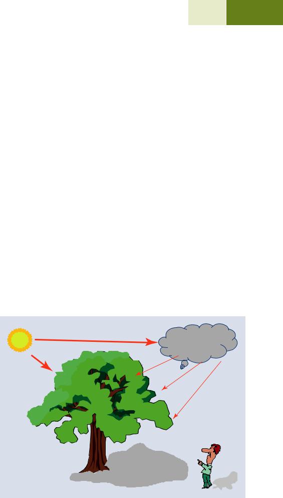
Establishing a Robust Light-Optical Analogy
The human visual process has developed in a world of top lighting (. Fig. 7.6): sunlight comes from above in the outdoors; our indoor environment is illuminated from light sources on the ceiling or lamp fixtures placed above our comfortable reading chair. We instinctively expect that brightly illuminated features must be facing upward to receive light from the source above, while poorly illuminated features are facing away from the light source. Thus, to establish the strongest possible light-optical analogy for the SEM/E–T (positive bias) image, we need to create a situation of apparent top lighting. Because the strong source of apparent illumination in an SEM image appears to come from the detector (direct BSEs, SE1, and SE2 for an E–T [positive bias] detector), by ensuring that the effective location of the E–T detector is at the top of the SEM image field as it is presented to the viewer, any feature facing the E–T detector will appear bright, thus establishing that the apparent lighting of the scene presented to the viewer will be from above. All features that can be reached by the electron beam will produce some signal, even those facing away from the E–T (positive bias) detector or that are screened by local topography, through the
Getting It Wrong: Breaking the Light-Optical Analogy of the Everhart–Thornley (Positive Bias) Detector
If the microscopist is not careful, it is possible to break the light-optical analogy of the Everhart-Thornley (positive bias) detector. This situation can arise through improper collection of the image by misuse of the feature called “Scan Rotation” (or in subsequent off-line image modification with image processing software). “Scan Rotation” is a commonly available feature of nearly all SEM systems that allows the microscopist to arbitrarily orient an image on the display screen. While this may seem to be a useful feature that enables the presentation of the features of a specimen in a more aesthetically pleasing manner (e.g., aligning a fiber along the long axis of a rectangular image), scan rotation changes the apparent position of the E–T detector (indeed, of all detectors) in the image with potentially serious consequences that can compromise the light-optical analogy of the E–T (positive bias) detector. The observer is naturally accustomed to having top illumination when interpreting images of topography, that is, the apparent source of illumination coming from the top of the field-of-view and shining
. Fig. 7.6 We have evolved in a world of top lighting. Features
facing the Sun are brightly illuminated, while features facing
away are shaded but receive some illumination from atmospheric scattering. Bright = facing upwards
118\ Chapter 7 · SEM Image Interpretation
a |
b |
|
|
10 mm |
10 mm |
7 |
|
||
|
|
||
|
|
|
|
|
c |
|
d |
|
|
10 mm |
10 mm |
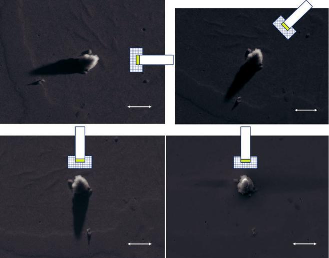
. Fig. 7.7 a SEM image of a particle on a surface as prepared with the E–T (negative bias) detector in the 90° clockwise position shown; E0 = 20 keV. Note strong shadowing pointing away from E–T . b SEM image of a particle on a surface as prepared with the E–T (negative bias) detector in the 45° clockwise position shown; E0 = 20 keV. Note strong shadowing pointing away from E–T . c SEM image of a particle
on a surface as prepared with the E–T (negative bias) detector in the 0° clockwise (12 o’clock) position shown; E0 = 20 keV. Note strong shadowing pointing away from E–T . d SEM image of a particle on a surface as prepared with the E–T (positive bias) detector in the 0° clockwise (12 o’clock) position shown; E0 = 20 keV. Note lack of shadowing but bright surface facing the E–T (positive bias) detector
down on the features of the specimen. When the top lighting condition is violated and the observer is unaware of the alteration of the scene illumination, then the sense of the topography can appear inverted. Arbitrary scan rotation can effectively place the E–T detector, or any other asymmetrically placed (i.e., off-axis) detector, at the bottom or sides of the image, and if the observer is unaware of this situation of unfamiliar illumination, misinterpretation of the specimen topography is likely to result. This is especially true in the case of specimens for which there are limited visual clues. For example, the SEM image of an insect contains many familiar features—e.g., head, eyes, legs, etc.—that make it almost impossible to invert the topography regardless of the
apparent lighting. By comparison, the image of an undulating surface of an unknown object may provide no clues that cause the proper sense of the topography to “click in” for the observer. Having top illumination is critical in such cases. When a microscopist works in a multi-user facility, the possibility must always be considered that a previous user may have arbitrarily adjusted the scan rotation. As part of a personal quality-assurance plan, the careful microscopist should confirm that the location of the E–T detector is at the top center of the image. . Figure 7.7 demonstrates a procedure that enables unambiguous location of the E–T detector. Some (but not all) implementations of the E–T detector enable the user to “deconstruct” the E–T detector image by

7.3 · Interpretation of SEM Images of Specimen Topography
selectively excluding the SE component of the total signal— either by changing the Faraday cage voltage to negative values to reject the very low energy SEs (e.g., −50 V cage bias) or by eliminating the high potential on the scintillator so that SEs cannot be accelerated to sufficient kinetic energy to excite scintillation. Even without the high potential applied to the scintillator, the E–T detector remains sensitive to the high energy BSEs generated by a high energy primary beam, for example., E0 ≥20 keV, which creates a large fraction of BSEs with energy >10 keV. As a passive scintillator or with the negative Faraday cage potential applied, the E–T (negative bias) detector only collects the small fraction of high energy BSEs scattered into the solid angle defined by the E–T scintillator. When the direct BSE mode of the E–T (negative bias) detector is selected, debris on a flat surface is found to create distinct shadows that point away from the apparent source of illumination, the E–T detector. By using the scan rotation, the effective position of the E–T detector can then be moved to the top of the image, as shown in the sequence of . Fig. 7.7a–c, thus achieving the desired top-lighting situation. When the conventional E–T (positive bias) is used to image this same field of view (. Fig. 7.7d), the strong shadow of the particle disappears because of the efficient collection of SEs, particularly the SE3 component, and now has a bright edge along the top which reinforces the impression that it rises above the general surface.
Note that physically rotating the specimen stage to change the angular relation of the specimen relative to the E–T (or any other) detector does not change the location of the apparent source of illumination in the displayed image. Rotating the specimen stage changes which specimen features are directed toward the detector, but the scan orientation on the displayed image determines the relative position of the detector in the image presented to the viewer and the apparent direction of the illumination.
Deconstructing the SEM/E–T Image of Topography
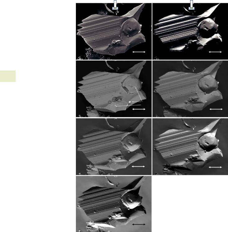
It is often useful to examine the separate SE and BSE components of the E–T detector image. An example of a blocky fragment of pyrite (FeS2) imaged with a positively-biased E–T detector is shown in . Fig. 7.8a. In this image, the effective position of the E–T detector relative to the presentation of the image is at the top center. . Figure 7.8b shows the same field of view with the Faraday cage biased negatively to exclude SEs so that only direct BSEs contribute to the SEM image. The image contrast is now extremely harsh, since topographic features facing toward the detector are illuminated, while those facing away are completely lost. Comparing
. Fig. 7.8a, b, the features that appear bright in the BSE-only image are also brighter in the full BSE + SE image obtained with the positively biased E–T detector, demonstrating the presence of the direct-BSE component. The much softer contrast of nearly all surfaces seen in the BSE + SE image of
119 |
|
7 |
|
|
|
. Fig. 7.8a demonstrates the efficiency of the E–T detector for collection of signal from virtually all surfaces of the specimen that the primary beam strikes.
7.3.3\ Imaging Specimen Topography
With a Semiconductor BSE Detector
A segmented (A and B semicircular segments) semiconductor BSE detector placed directly above the specimen is illustrated schematically in . Fig. 7.9. This BSE detector is mounted below the final lens and is placed symmetrically around the beam, so that in the summation mode it acts as an annular detector. A simple topographic specimen is illustrated, oriented so that the left face directs BSEs toward the A-segment, while the right face directs BSEs toward the B-segment. This A and B detector pair is typically arranged so that one of the segments, “A,” is oriented so that it appears to illuminate from the top of the image, while the “B” segment appears to illuminate from the bottom of the image. The segmented detector enables selection of several modes of operation: SUM mode (A + B), DIFFERENCE mode (A−B), and individual detectors A or B) (Kimoto and Hashimoto 1966).
SUM Mode (A + B)
The two-segment semiconductor BSE detector operating in the summation (A + B) mode was used to image the same pyrite specimen previously imaged with the E–T (positive bias) and E–T (negative bias), as shown in . Fig. 7.8c. The placement of the large solid angle BSE is so close to the primary electron beam that it creates the effect of apparent wide-angle illumination that is highly directional along the line-of-sight of the observer, which would be the light-optical equivalent of being inside a flashlight looking along the beam. With such directional illumination along the observer’s line-of-sight, the brightest topographic features are those oriented perpendicular to the line-of-sight, while tilted surfaces appear darker, resulting in a substantially different impression of the topography of the pyrite specimen compared to the E–T (positive bias) image in . Fig. 7.8a. The large solid angle of the detector acts to suppress topographic contrast, since local differences in the directionality of BSE emission caused by differently inclined surfaces are effectively eliminated when the diverging BSEs are intercepted by another part of the large BSE detector.
Another effect that is observed in the A + B image is the class of very bright inclusions which were subsequently determined to be galena (PbS) by X-ray microanalysis. The large difference in average atomic number between FeS2
(Zav = 20.7) and PbS (Zav = 73.2) results in strong atomic number (compositional) between the PbS inclusions and the FeS2 matrix. Although there is a significant BSE signal component in the E–T (positive bias) image in . Fig. 7.8a, the
120\ Chapter 7 · SEM Image Interpretation
. Fig. 7.8 a SEM/E–T (positive bias) image of a fractured fragment of pyrite; E0 = 20 keV. b SEM/E–T (negative bias) image of a fractured fragment of pyrite; E0 = 20 keV. c SEM/BSE (A + B) SUM-mode image of a fractured fragment of pyrite; E0 = 20 keV. d SEM/BSE (A segment) image (detector at top of image field) of a fractured fragment of pyrite (FeS2); E0 = 20 keV. e SEM/BSE
(B segment) image (detector at bottom of image field) of a fractured fragment of pyrite (FeS2); E0 = 20 keV. f SEM/BSE (A−B) image (detector DIFFERENCE image) of a fractured fragment
7 of pyrite (FeS2); E0 = 20 keV. g SEM/BSE (B−A) image (detector DIFFERENCE image) of a fractured fragment of pyrite (FeS2); E0 = 20 keV
a
BSE SUM A+B
c
e
b
50 mm
d
Pbs inclusions
50 mm
BSE DIFFERENCE A-B
f
50 mm
BSE B segment
BSE DIFFERENCE B-A BSE A segment
g
50 mm
BSE B segment
50 mm
BSE A segment
50 mm
BSE A segment
50 mm
BSE B segment
topographic contrast is so strong that it overwhelms the compositional contrast.
Examining Images Prepared
With the Individual Detector Segments
Some semiconductor BSE detector systems enable the microscopist to view BSE images prepared with the signal derived from the individual components of a segmented
detector. As illustrated in . Fig. 7.9 for a two-segment BSE detector, the individual segments effectively provide an off- axis, asymmetric illumination of the specimen. Comparing the A-segment and B-segment images of the pyrite crystal in
. Fig. 7.8d, e, the features facing each detector can be discerned and a sense of the topography can be obtained by comparing the two images. But note the strong effect of the apparent inversion of the sense of the topography in the