- •Preface
- •Imaging Microscopic Features
- •Measuring the Crystal Structure
- •References
- •Contents
- •1.4 Simulating the Effects of Elastic Scattering: Monte Carlo Calculations
- •What Are the Main Features of the Beam Electron Interaction Volume?
- •How Does the Interaction Volume Change with Composition?
- •How Does the Interaction Volume Change with Incident Beam Energy?
- •How Does the Interaction Volume Change with Specimen Tilt?
- •1.5 A Range Equation To Estimate the Size of the Interaction Volume
- •References
- •2: Backscattered Electrons
- •2.1 Origin
- •2.2.1 BSE Response to Specimen Composition (η vs. Atomic Number, Z)
- •SEM Image Contrast with BSE: “Atomic Number Contrast”
- •SEM Image Contrast: “BSE Topographic Contrast—Number Effects”
- •2.2.3 Angular Distribution of Backscattering
- •Beam Incident at an Acute Angle to the Specimen Surface (Specimen Tilt > 0°)
- •SEM Image Contrast: “BSE Topographic Contrast—Trajectory Effects”
- •2.2.4 Spatial Distribution of Backscattering
- •Depth Distribution of Backscattering
- •Radial Distribution of Backscattered Electrons
- •2.3 Summary
- •References
- •3: Secondary Electrons
- •3.1 Origin
- •3.2 Energy Distribution
- •3.3 Escape Depth of Secondary Electrons
- •3.8 Spatial Characteristics of Secondary Electrons
- •References
- •4: X-Rays
- •4.1 Overview
- •4.2 Characteristic X-Rays
- •4.2.1 Origin
- •4.2.2 Fluorescence Yield
- •4.2.3 X-Ray Families
- •4.2.4 X-Ray Nomenclature
- •4.2.6 Characteristic X-Ray Intensity
- •Isolated Atoms
- •X-Ray Production in Thin Foils
- •X-Ray Intensity Emitted from Thick, Solid Specimens
- •4.3 X-Ray Continuum (bremsstrahlung)
- •4.3.1 X-Ray Continuum Intensity
- •4.3.3 Range of X-ray Production
- •4.4 X-Ray Absorption
- •4.5 X-Ray Fluorescence
- •References
- •5.1 Electron Beam Parameters
- •5.2 Electron Optical Parameters
- •5.2.1 Beam Energy
- •Landing Energy
- •5.2.2 Beam Diameter
- •5.2.3 Beam Current
- •5.2.4 Beam Current Density
- •5.2.5 Beam Convergence Angle, α
- •5.2.6 Beam Solid Angle
- •5.2.7 Electron Optical Brightness, β
- •Brightness Equation
- •5.2.8 Focus
- •Astigmatism
- •5.3 SEM Imaging Modes
- •5.3.1 High Depth-of-Field Mode
- •5.3.2 High-Current Mode
- •5.3.3 Resolution Mode
- •5.3.4 Low-Voltage Mode
- •5.4 Electron Detectors
- •5.4.1 Important Properties of BSE and SE for Detector Design and Operation
- •Abundance
- •Angular Distribution
- •Kinetic Energy Response
- •5.4.2 Detector Characteristics
- •Angular Measures for Electron Detectors
- •Elevation (Take-Off) Angle, ψ, and Azimuthal Angle, ζ
- •Solid Angle, Ω
- •Energy Response
- •Bandwidth
- •5.4.3 Common Types of Electron Detectors
- •Backscattered Electrons
- •Passive Detectors
- •Scintillation Detectors
- •Semiconductor BSE Detectors
- •5.4.4 Secondary Electron Detectors
- •Everhart–Thornley Detector
- •Through-the-Lens (TTL) Electron Detectors
- •TTL SE Detector
- •TTL BSE Detector
- •Measuring the DQE: BSE Semiconductor Detector
- •References
- •6: Image Formation
- •6.1 Image Construction by Scanning Action
- •6.2 Magnification
- •6.3 Making Dimensional Measurements With the SEM: How Big Is That Feature?
- •Using a Calibrated Structure in ImageJ-Fiji
- •6.4 Image Defects
- •6.4.1 Projection Distortion (Foreshortening)
- •6.4.2 Image Defocusing (Blurring)
- •6.5 Making Measurements on Surfaces With Arbitrary Topography: Stereomicroscopy
- •6.5.1 Qualitative Stereomicroscopy
- •Fixed beam, Specimen Position Altered
- •Fixed Specimen, Beam Incidence Angle Changed
- •6.5.2 Quantitative Stereomicroscopy
- •Measuring a Simple Vertical Displacement
- •References
- •7: SEM Image Interpretation
- •7.1 Information in SEM Images
- •7.2.2 Calculating Atomic Number Contrast
- •Establishing a Robust Light-Optical Analogy
- •Getting It Wrong: Breaking the Light-Optical Analogy of the Everhart–Thornley (Positive Bias) Detector
- •Deconstructing the SEM/E–T Image of Topography
- •SUM Mode (A + B)
- •DIFFERENCE Mode (A−B)
- •References
- •References
- •9: Image Defects
- •9.1 Charging
- •9.1.1 What Is Specimen Charging?
- •9.1.3 Techniques to Control Charging Artifacts (High Vacuum Instruments)
- •Observing Uncoated Specimens
- •Coating an Insulating Specimen for Charge Dissipation
- •Choosing the Coating for Imaging Morphology
- •9.2 Radiation Damage
- •9.3 Contamination
- •References
- •10: High Resolution Imaging
- •10.2 Instrumentation Considerations
- •10.4.1 SE Range Effects Produce Bright Edges (Isolated Edges)
- •10.4.4 Too Much of a Good Thing: The Bright Edge Effect Hinders Locating the True Position of an Edge for Critical Dimension Metrology
- •10.5.1 Beam Energy Strategies
- •Low Beam Energy Strategy
- •High Beam Energy Strategy
- •Making More SE1: Apply a Thin High-δ Metal Coating
- •Making Fewer BSEs, SE2, and SE3 by Eliminating Bulk Scattering From the Substrate
- •10.6 Factors That Hinder Achieving High Resolution
- •10.6.2 Pathological Specimen Behavior
- •Contamination
- •Instabilities
- •References
- •11: Low Beam Energy SEM
- •11.3 Selecting the Beam Energy to Control the Spatial Sampling of Imaging Signals
- •11.3.1 Low Beam Energy for High Lateral Resolution SEM
- •11.3.2 Low Beam Energy for High Depth Resolution SEM
- •11.3.3 Extremely Low Beam Energy Imaging
- •References
- •12.1.1 Stable Electron Source Operation
- •12.1.2 Maintaining Beam Integrity
- •12.1.4 Minimizing Contamination
- •12.3.1 Control of Specimen Charging
- •12.5 VPSEM Image Resolution
- •References
- •13: ImageJ and Fiji
- •13.1 The ImageJ Universe
- •13.2 Fiji
- •13.3 Plugins
- •13.4 Where to Learn More
- •References
- •14: SEM Imaging Checklist
- •14.1.1 Conducting or Semiconducting Specimens
- •14.1.2 Insulating Specimens
- •14.2 Electron Signals Available
- •14.2.1 Beam Electron Range
- •14.2.2 Backscattered Electrons
- •14.2.3 Secondary Electrons
- •14.3 Selecting the Electron Detector
- •14.3.2 Backscattered Electron Detectors
- •14.3.3 “Through-the-Lens” Detectors
- •14.4 Selecting the Beam Energy for SEM Imaging
- •14.4.4 High Resolution SEM Imaging
- •Strategy 1
- •Strategy 2
- •14.5 Selecting the Beam Current
- •14.5.1 High Resolution Imaging
- •14.5.2 Low Contrast Features Require High Beam Current and/or Long Frame Time to Establish Visibility
- •14.6 Image Presentation
- •14.6.1 “Live” Display Adjustments
- •14.6.2 Post-Collection Processing
- •14.7 Image Interpretation
- •14.7.1 Observer’s Point of View
- •14.7.3 Contrast Encoding
- •14.8.1 VPSEM Advantages
- •14.8.2 VPSEM Disadvantages
- •15: SEM Case Studies
- •15.1 Case Study: How High Is That Feature Relative to Another?
- •15.2 Revealing Shallow Surface Relief
- •16.1.2 Minor Artifacts: The Si-Escape Peak
- •16.1.3 Minor Artifacts: Coincidence Peaks
- •16.1.4 Minor Artifacts: Si Absorption Edge and Si Internal Fluorescence Peak
- •16.2 “Best Practices” for Electron-Excited EDS Operation
- •16.2.1 Operation of the EDS System
- •Choosing the EDS Time Constant (Resolution and Throughput)
- •Choosing the Solid Angle of the EDS
- •Selecting a Beam Current for an Acceptable Level of System Dead-Time
- •16.3.1 Detector Geometry
- •16.3.2 Process Time
- •16.3.3 Optimal Working Distance
- •16.3.4 Detector Orientation
- •16.3.5 Count Rate Linearity
- •16.3.6 Energy Calibration Linearity
- •16.3.7 Other Items
- •16.3.8 Setting Up a Quality Control Program
- •Using the QC Tools Within DTSA-II
- •Creating a QC Project
- •Linearity of Output Count Rate with Live-Time Dose
- •Resolution and Peak Position Stability with Count Rate
- •Solid Angle for Low X-ray Flux
- •Maximizing Throughput at Moderate Resolution
- •References
- •17: DTSA-II EDS Software
- •17.1 Getting Started With NIST DTSA-II
- •17.1.1 Motivation
- •17.1.2 Platform
- •17.1.3 Overview
- •17.1.4 Design
- •Simulation
- •Quantification
- •Experiment Design
- •Modeled Detectors (. Fig. 17.1)
- •Window Type (. Fig. 17.2)
- •The Optimal Working Distance (. Figs. 17.3 and 17.4)
- •Elevation Angle
- •Sample-to-Detector Distance
- •Detector Area
- •Crystal Thickness
- •Number of Channels, Energy Scale, and Zero Offset
- •Resolution at Mn Kα (Approximate)
- •Azimuthal Angle
- •Gold Layer, Aluminum Layer, Nickel Layer
- •Dead Layer
- •Zero Strobe Discriminator (. Figs. 17.7 and 17.8)
- •Material Editor Dialog (. Figs. 17.9, 17.10, 17.11, 17.12, 17.13, and 17.14)
- •17.2.1 Introduction
- •17.2.2 Monte Carlo Simulation
- •17.2.4 Optional Tables
- •References
- •18: Qualitative Elemental Analysis by Energy Dispersive X-Ray Spectrometry
- •18.1 Quality Assurance Issues for Qualitative Analysis: EDS Calibration
- •18.2 Principles of Qualitative EDS Analysis
- •Exciting Characteristic X-Rays
- •Fluorescence Yield
- •X-ray Absorption
- •Si Escape Peak
- •Coincidence Peaks
- •18.3 Performing Manual Qualitative Analysis
- •Beam Energy
- •Choosing the EDS Resolution (Detector Time Constant)
- •Obtaining Adequate Counts
- •18.4.1 Employ the Available Software Tools
- •18.4.3 Lower Photon Energy Region
- •18.4.5 Checking Your Work
- •18.5 A Worked Example of Manual Peak Identification
- •References
- •19.1 What Is a k-ratio?
- •19.3 Sets of k-ratios
- •19.5 The Analytical Total
- •19.6 Normalization
- •19.7.1 Oxygen by Assumed Stoichiometry
- •19.7.3 Element by Difference
- •19.8 Ways of Reporting Composition
- •19.8.1 Mass Fraction
- •19.8.2 Atomic Fraction
- •19.8.3 Stoichiometry
- •19.8.4 Oxide Fractions
- •Example Calculations
- •19.9 The Accuracy of Quantitative Electron-Excited X-ray Microanalysis
- •19.9.1 Standards-Based k-ratio Protocol
- •19.9.2 “Standardless Analysis”
- •19.10 Appendix
- •19.10.1 The Need for Matrix Corrections To Achieve Quantitative Analysis
- •19.10.2 The Physical Origin of Matrix Effects
- •19.10.3 ZAF Factors in Microanalysis
- •X-ray Generation With Depth, φ(ρz)
- •X-ray Absorption Effect, A
- •X-ray Fluorescence, F
- •References
- •20.2 Instrumentation Requirements
- •20.2.1 Choosing the EDS Parameters
- •EDS Spectrum Channel Energy Width and Spectrum Energy Span
- •EDS Time Constant (Resolution and Throughput)
- •EDS Calibration
- •EDS Solid Angle
- •20.2.2 Choosing the Beam Energy, E0
- •20.2.3 Measuring the Beam Current
- •20.2.4 Choosing the Beam Current
- •Optimizing Analysis Strategy
- •20.3.4 Ba-Ti Interference in BaTiSi3O9
- •20.4 The Need for an Iterative Qualitative and Quantitative Analysis Strategy
- •20.4.2 Analysis of a Stainless Steel
- •20.5 Is the Specimen Homogeneous?
- •20.6 Beam-Sensitive Specimens
- •20.6.1 Alkali Element Migration
- •20.6.2 Materials Subject to Mass Loss During Electron Bombardment—the Marshall-Hall Method
- •Thin Section Analysis
- •Bulk Biological and Organic Specimens
- •References
- •21: Trace Analysis by SEM/EDS
- •21.1 Limits of Detection for SEM/EDS Microanalysis
- •21.2.1 Estimating CDL from a Trace or Minor Constituent from Measuring a Known Standard
- •21.2.2 Estimating CDL After Determination of a Minor or Trace Constituent with Severe Peak Interference from a Major Constituent
- •21.3 Measurements of Trace Constituents by Electron-Excited Energy Dispersive X-ray Spectrometry
- •The Inevitable Physics of Remote Excitation Within the Specimen: Secondary Fluorescence Beyond the Electron Interaction Volume
- •Simulation of Long-Range Secondary X-ray Fluorescence
- •NIST DTSA II Simulation: Vertical Interface Between Two Regions of Different Composition in a Flat Bulk Target
- •NIST DTSA II Simulation: Cubic Particle Embedded in a Bulk Matrix
- •21.5 Summary
- •References
- •22.1.2 Low Beam Energy Analysis Range
- •22.2 Advantage of Low Beam Energy X-Ray Microanalysis
- •22.2.1 Improved Spatial Resolution
- •22.3 Challenges and Limitations of Low Beam Energy X-Ray Microanalysis
- •22.3.1 Reduced Access to Elements
- •22.3.3 At Low Beam Energy, Almost Everything Is Found To Be Layered
- •Analysis of Surface Contamination
- •References
- •23: Analysis of Specimens with Special Geometry: Irregular Bulk Objects and Particles
- •23.2.1 No Chemical Etching
- •23.3 Consequences of Attempting Analysis of Bulk Materials With Rough Surfaces
- •23.4.1 The Raw Analytical Total
- •23.4.2 The Shape of the EDS Spectrum
- •23.5 Best Practices for Analysis of Rough Bulk Samples
- •23.6 Particle Analysis
- •Particle Sample Preparation: Bulk Substrate
- •The Importance of Beam Placement
- •Overscanning
- •“Particle Mass Effect”
- •“Particle Absorption Effect”
- •The Analytical Total Reveals the Impact of Particle Effects
- •Does Overscanning Help?
- •23.6.6 Peak-to-Background (P/B) Method
- •Specimen Geometry Severely Affects the k-ratio, but Not the P/B
- •Using the P/B Correspondence
- •23.7 Summary
- •References
- •24: Compositional Mapping
- •24.2 X-Ray Spectrum Imaging
- •24.2.1 Utilizing XSI Datacubes
- •24.2.2 Derived Spectra
- •SUM Spectrum
- •MAXIMUM PIXEL Spectrum
- •24.3 Quantitative Compositional Mapping
- •24.4 Strategy for XSI Elemental Mapping Data Collection
- •24.4.1 Choosing the EDS Dead-Time
- •24.4.2 Choosing the Pixel Density
- •24.4.3 Choosing the Pixel Dwell Time
- •“Flash Mapping”
- •High Count Mapping
- •References
- •25.1 Gas Scattering Effects in the VPSEM
- •25.1.1 Why Doesn’t the EDS Collimator Exclude the Remote Skirt X-Rays?
- •25.2 What Can Be Done To Minimize gas Scattering in VPSEM?
- •25.2.2 Favorable Sample Characteristics
- •Particle Analysis
- •25.2.3 Unfavorable Sample Characteristics
- •References
- •26.1 Instrumentation
- •26.1.2 EDS Detector
- •26.1.3 Probe Current Measurement Device
- •Direct Measurement: Using a Faraday Cup and Picoammeter
- •A Faraday Cup
- •Electrically Isolated Stage
- •Indirect Measurement: Using a Calibration Spectrum
- •26.1.4 Conductive Coating
- •26.2 Sample Preparation
- •26.2.1 Standard Materials
- •26.2.2 Peak Reference Materials
- •26.3 Initial Set-Up
- •26.3.1 Calibrating the EDS Detector
- •Selecting a Pulse Process Time Constant
- •Energy Calibration
- •Quality Control
- •Sample Orientation
- •Detector Position
- •Probe Current
- •26.4 Collecting Data
- •26.4.1 Exploratory Spectrum
- •26.4.2 Experiment Optimization
- •26.4.3 Selecting Standards
- •26.4.4 Reference Spectra
- •26.4.5 Collecting Standards
- •26.4.6 Collecting Peak-Fitting References
- •26.5 Data Analysis
- •26.5.2 Quantification
- •26.6 Quality Check
- •Reference
- •27.2 Case Study: Aluminum Wire Failures in Residential Wiring
- •References
- •28: Cathodoluminescence
- •28.1 Origin
- •28.2 Measuring Cathodoluminescence
- •28.3 Applications of CL
- •28.3.1 Geology
- •Carbonado Diamond
- •Ancient Impact Zircons
- •28.3.2 Materials Science
- •Semiconductors
- •Lead-Acid Battery Plate Reactions
- •28.3.3 Organic Compounds
- •References
- •29.1.1 Single Crystals
- •29.1.2 Polycrystalline Materials
- •29.1.3 Conditions for Detecting Electron Channeling Contrast
- •Specimen Preparation
- •Instrument Conditions
- •29.2.1 Origin of EBSD Patterns
- •29.2.2 Cameras for EBSD Pattern Detection
- •29.2.3 EBSD Spatial Resolution
- •29.2.5 Steps in Typical EBSD Measurements
- •Sample Preparation for EBSD
- •Align Sample in the SEM
- •Check for EBSD Patterns
- •Adjust SEM and Select EBSD Map Parameters
- •Run the Automated Map
- •29.2.6 Display of the Acquired Data
- •29.2.7 Other Map Components
- •29.2.10 Application Example
- •Application of EBSD To Understand Meteorite Formation
- •29.2.11 Summary
- •Specimen Considerations
- •EBSD Detector
- •Selection of Candidate Crystallographic Phases
- •Microscope Operating Conditions and Pattern Optimization
- •Selection of EBSD Acquisition Parameters
- •Collect the Orientation Map
- •References
- •30.1 Introduction
- •30.2 Ion–Solid Interactions
- •30.3 Focused Ion Beam Systems
- •30.5 Preparation of Samples for SEM
- •30.5.1 Cross-Section Preparation
- •30.5.2 FIB Sample Preparation for 3D Techniques and Imaging
- •30.6 Summary
- •References
- •31: Ion Beam Microscopy
- •31.1 What Is So Useful About Ions?
- •31.2 Generating Ion Beams
- •31.3 Signal Generation in the HIM
- •31.5 Patterning with Ion Beams
- •31.7 Chemical Microanalysis with Ion Beams
- •References
- •Appendix
- •A Database of Electron–Solid Interactions
- •Introduction
- •Backscattered Electrons
- •Secondary Yields
- •Stopping Powers
- •X-ray Ionization Cross Sections
- •Conclusions
- •References
- •Index
- •Reference List
- •Index
95 |
6 |
6.3 · Making Dimensional Measurements With the SEM: How Big Is That Feature?
ments or “pixels” of number n along an edge. The specimen pixel edge dimension is given by
Specimen pixel dimension = l / n \ |
(6.1) |
With equal values of the scan l along the x- and y-dimensions, the pixels will be square. Strictly, the pixel is the geometric center of the area defined by the edges given by Eq. (6.1), and the center-to-center spacing or pitch is given by Eq. (6.1). In creating an SEM image, the center of the beam is placed in the center of a specific pixel, dwells for a specific time, tp, and the signal information Isig from various sources “j”—e.g., SE, BSE, X-ray, etc.—collected during that time at that (x, y) location is stored at a corresponding location in a data matrix with a minimum of three dimensions (x, y, Ij). The final image viewed by the microscopist is created by reading the stored data matrix into a corresponding pattern of (x, y) display pixels with a total edge dimension L, and adjusting the display brightness (“gray level”, varying from black to white) according to the relative strength of the measured signal(s).
6.2\ Magnification
“Magnification” in such a scanning system is given by the ratio of the edge dimensions of the specimen area and the display area:
M =L / l \ |
(6.2) |
Since the final display size is typically fixed, increasing the magnification in this scanning system means that the edge dimension of the area scanned on the specimen is reduced.
6.2.1\ Magnification, Image Dimensions,
and Scale Bars
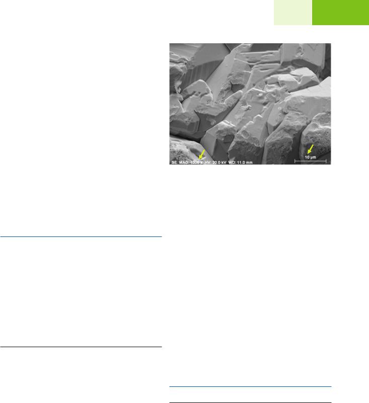
One of the most important pieces of information that the microscopist seeks is the size of objects of interest. The first step in determining the size of an object is knowledge of the parameters in Eq. (6.2): the linear edge length of the area scanned on the specimen and on the display. The nominal SEM magnification appropriate to the display as viewed by the microscopist is typically embedded in the alphanumeric record that appears with the image as presented on most SEMs, as shown in the example of . Fig. 6.3, and as recorded with the metadata associated with the digital record of the image. “Magnification” only has a useful meaning for the display on which the original image was viewed, since this is the display for which L in Eq. (6.2) is strictly valid. If the image is transferred to another display with a different value of L, for example, projected on a large screen, then the specific magnification value embedded in the metadata bar becomes meaningless. Much more meaningful are the x- and y-image dimensions, which are the lengths of the orthogonal boundaries of the scanned square area on the specimen,
Nominal |
Scale bar |
magnification |
|
. Fig. 6.3 SEM-SE image of silver crystals showing a typical information bar specifying the electron detector, the nominal magnification, the accelerating voltage, and a scale bar
l, in . Fig. 6.2, or for rectangular images, the dimensions in orthogonal directions, l by k (dimensions: millimeters, micrometers, or nanometers, as appropriate). While the image dimension(s) is a much more robust term that automatically scales with the presentation of the image, this term is also vulnerable to inadvertent mistakes, such as might happen if the image is “cropped,” either digitally or manually in hard copy and the appropriate reduction in size is not recorded by modifying l (and k, if rectangular) appropriately. The most robust measure in terms of image integrity is the dimensional scale bar, which shows the length that corresponds to a specific millimeter, micrometer, or nanometer measure. Because this feature is embedded directly in the image (as well as in the metadata associated with the image), it cannot be lost unless the image is severely (and obviously) cropped. Such a scale bar automatically enlarges or contracts as the image size is modified for subsequent publication or projection.
6.3\ Making Dimensional Measurements With the SEM: How Big Is That Feature?
6.3.1\ Calibrating theImage
The validity of the dimensional marker displayed on the SEM image should not be automatically assumed (Postek et al. 2014). As part of a laboratory quality-assurance program, the dimensional marker and/or the x- and y-dimensions of the scanned field should be calibrated and the calibration periodically confirmed. This can be accomplished with a “scale calibration artifact,” a specimen that contains features with various defined spacings whose dimensions are traceable to the fundamental primary length standard through a national measurement institution. An example of such a scale calibration artifact suitable for SEM is Reference Material RM 8820 (Postek et al. 2014; National Institute of Standards and
\96
a
6
b NIST
Chapter 6 ·
G
Image Formation
G |
F |
E |
NIST RM 8820 SEM scale calibration artifact:
(lithographically patterned silicon chip, 20 mm by 20 mm)
NIST
1000 m
750 m
500 m
250 m
|
|
|
|
|
100 m |
|
|
|
|
2 |
50 m |
|
|
|
|
|
1 |
|
|
|
|
NIST |
|
|
|
|
|
|
1500 m |
|
|
|
|
NIST |
|
|
|
|
|
3 |
A: 200 nm pitch |
|
|
|
|
|
|
D |
C |
B |
A |
4 |
B: 280 nm pitch |
|
|
||||
|
|
|
|
A |
C: 400 nm pitch |
|
|
|
|
D: 500 nm pitch |
|
|
|
|
|
|
NIST 3 4
NIST
1500 m
|
F |
B |
E: 700 nm pitch |
|
|
|
|
||
|
E |
C |
F: 1 µm pitch |
|
|
|
|||
|
D |
D |
G: 2 µm pitch |
|
|
C |
E |
|
|
|
B |
F |
The center area is filled |
|
|
|
|
||
|
A |
G |
with 1 µm crosses on |
|
|
|
|||
|
A B C D E F |
G |
non-connected structures |
|
2 |
and with a 1 µm grid on |
|||
|
|
|||
1 |
1 |
|
connected structures |
|
|
|
|
NIST |
NIST
10 m
4 m
++
++
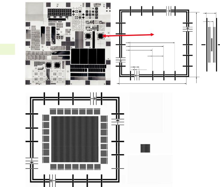
. Fig. 6.4 a Scale calibration artifact Reference Material 8820 (National Institute of Standards and Technology, U.S.) (From Postek et al. 2014). b Detail within the feature noted in . Fig. 6.4a (From Postek et al. 2014)
Technology [USA]), shown in . Fig. 6.4. This scale calibration artifact consists of an elaborate collection of linear features produced by lithography on a silicon substrate. It is important to calibrate the SEM over the full range of magnifications to be used for subsequent work. RM 8820 contains large-scale structures suitable for low and intermediate magnifications, for example, a span of 1500 μm (1.5 mm) as indicated by the red arrows in . Fig. 6.4a, that permit calibration of scan fields ranging up to 1 × 1 cm (e.g., a nominal
magnification of 10× on a 10 x 10-cm display). Scanned fields as small as 1 × 1 μm (e.g., a nominal magnification of 100,000×) can be calibrated with the series of structures with pitches of various repeat distances shown in . Fig. 6.4b. The structures present in RM 8820 enable simultaneous calibration along the x- and y-axes of the image so that image distortion can be minimized. Accurate calibration in orthogonal directions is critical for establishing “square pixels” in order to avoid introducing serious distortions into the scanned image.
6.3 · Making Dimensional Measurements With the SEM: How Big Is That Feature?
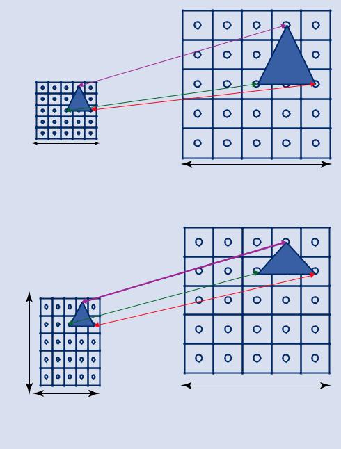
. Fig. 6.5 a Careful calibration of the x- and y-scans produces square pixels, and a faithful reproduction of shapes lying in the scan plane perpendicular to the optic axis. b Distortion in the display of an object caused by nonsquare pixels in the image scan
a
l
Beam locations on specimen and specimen pixels
l
b
l'
l
Beam locations on specimen and specimen pixels
97 |
|
6 |
|
|
|
L
Beam locations in computer memory and display pixels
L
Beam locations in computer memory and display pixels
With square pixels, the shape of an object is faithfully transferred, as shown in . Fig. 6.5a, while non-square pixels in the specimen scan result in distortion in the displayed image,
. Fig. 6.5b.
Note that for all measurements the calibration artifact must be placed normal to the optic axis of the SEM to eliminate image foreshortening effects (see further discussion below).
Using a Calibrated Structure in ImageJ-Fiji
The image-processing software engine ImageJ-Fiji includes a “Set Scale” function that enables a user to transfer the image calibration to subsequent measurements made with various
functions. As shown in . Fig. 6.6a, starting with an image of a primary or secondary calibration artifact (i.e., where “secondary” refers to a commercial vendor artifact that is traceable to a primary national measurement calibration artifact) that contains a set of defined distances, the user can specify a vector that spans a particular pitch to establish the calibration at that magnification setting. This calibration procedure should then be repeated to cover the range of magnification settings to be used for subsequent measurements of unknowns. Note that the calibration that has been performed is only strictly valid for the SEM working distance at which the calibration artifact has been imaged. When a