

- •Preface
- •Imaging Microscopic Features
- •Measuring the Crystal Structure
- •References
- •Contents
- •1.4 Simulating the Effects of Elastic Scattering: Monte Carlo Calculations
- •What Are the Main Features of the Beam Electron Interaction Volume?
- •How Does the Interaction Volume Change with Composition?
- •How Does the Interaction Volume Change with Incident Beam Energy?
- •How Does the Interaction Volume Change with Specimen Tilt?
- •1.5 A Range Equation To Estimate the Size of the Interaction Volume
- •References
- •2: Backscattered Electrons
- •2.1 Origin
- •2.2.1 BSE Response to Specimen Composition (η vs. Atomic Number, Z)
- •SEM Image Contrast with BSE: “Atomic Number Contrast”
- •SEM Image Contrast: “BSE Topographic Contrast—Number Effects”
- •2.2.3 Angular Distribution of Backscattering
- •Beam Incident at an Acute Angle to the Specimen Surface (Specimen Tilt > 0°)
- •SEM Image Contrast: “BSE Topographic Contrast—Trajectory Effects”
- •2.2.4 Spatial Distribution of Backscattering
- •Depth Distribution of Backscattering
- •Radial Distribution of Backscattered Electrons
- •2.3 Summary
- •References
- •3: Secondary Electrons
- •3.1 Origin
- •3.2 Energy Distribution
- •3.3 Escape Depth of Secondary Electrons
- •3.8 Spatial Characteristics of Secondary Electrons
- •References
- •4: X-Rays
- •4.1 Overview
- •4.2 Characteristic X-Rays
- •4.2.1 Origin
- •4.2.2 Fluorescence Yield
- •4.2.3 X-Ray Families
- •4.2.4 X-Ray Nomenclature
- •4.2.6 Characteristic X-Ray Intensity
- •Isolated Atoms
- •X-Ray Production in Thin Foils
- •X-Ray Intensity Emitted from Thick, Solid Specimens
- •4.3 X-Ray Continuum (bremsstrahlung)
- •4.3.1 X-Ray Continuum Intensity
- •4.3.3 Range of X-ray Production
- •4.4 X-Ray Absorption
- •4.5 X-Ray Fluorescence
- •References
- •5.1 Electron Beam Parameters
- •5.2 Electron Optical Parameters
- •5.2.1 Beam Energy
- •Landing Energy
- •5.2.2 Beam Diameter
- •5.2.3 Beam Current
- •5.2.4 Beam Current Density
- •5.2.5 Beam Convergence Angle, α
- •5.2.6 Beam Solid Angle
- •5.2.7 Electron Optical Brightness, β
- •Brightness Equation
- •5.2.8 Focus
- •Astigmatism
- •5.3 SEM Imaging Modes
- •5.3.1 High Depth-of-Field Mode
- •5.3.2 High-Current Mode
- •5.3.3 Resolution Mode
- •5.3.4 Low-Voltage Mode
- •5.4 Electron Detectors
- •5.4.1 Important Properties of BSE and SE for Detector Design and Operation
- •Abundance
- •Angular Distribution
- •Kinetic Energy Response
- •5.4.2 Detector Characteristics
- •Angular Measures for Electron Detectors
- •Elevation (Take-Off) Angle, ψ, and Azimuthal Angle, ζ
- •Solid Angle, Ω
- •Energy Response
- •Bandwidth
- •5.4.3 Common Types of Electron Detectors
- •Backscattered Electrons
- •Passive Detectors
- •Scintillation Detectors
- •Semiconductor BSE Detectors
- •5.4.4 Secondary Electron Detectors
- •Everhart–Thornley Detector
- •Through-the-Lens (TTL) Electron Detectors
- •TTL SE Detector
- •TTL BSE Detector
- •Measuring the DQE: BSE Semiconductor Detector
- •References
- •6: Image Formation
- •6.1 Image Construction by Scanning Action
- •6.2 Magnification
- •6.3 Making Dimensional Measurements With the SEM: How Big Is That Feature?
- •Using a Calibrated Structure in ImageJ-Fiji
- •6.4 Image Defects
- •6.4.1 Projection Distortion (Foreshortening)
- •6.4.2 Image Defocusing (Blurring)
- •6.5 Making Measurements on Surfaces With Arbitrary Topography: Stereomicroscopy
- •6.5.1 Qualitative Stereomicroscopy
- •Fixed beam, Specimen Position Altered
- •Fixed Specimen, Beam Incidence Angle Changed
- •6.5.2 Quantitative Stereomicroscopy
- •Measuring a Simple Vertical Displacement
- •References
- •7: SEM Image Interpretation
- •7.1 Information in SEM Images
- •7.2.2 Calculating Atomic Number Contrast
- •Establishing a Robust Light-Optical Analogy
- •Getting It Wrong: Breaking the Light-Optical Analogy of the Everhart–Thornley (Positive Bias) Detector
- •Deconstructing the SEM/E–T Image of Topography
- •SUM Mode (A + B)
- •DIFFERENCE Mode (A−B)
- •References
- •References
- •9: Image Defects
- •9.1 Charging
- •9.1.1 What Is Specimen Charging?
- •9.1.3 Techniques to Control Charging Artifacts (High Vacuum Instruments)
- •Observing Uncoated Specimens
- •Coating an Insulating Specimen for Charge Dissipation
- •Choosing the Coating for Imaging Morphology
- •9.2 Radiation Damage
- •9.3 Contamination
- •References
- •10: High Resolution Imaging
- •10.2 Instrumentation Considerations
- •10.4.1 SE Range Effects Produce Bright Edges (Isolated Edges)
- •10.4.4 Too Much of a Good Thing: The Bright Edge Effect Hinders Locating the True Position of an Edge for Critical Dimension Metrology
- •10.5.1 Beam Energy Strategies
- •Low Beam Energy Strategy
- •High Beam Energy Strategy
- •Making More SE1: Apply a Thin High-δ Metal Coating
- •Making Fewer BSEs, SE2, and SE3 by Eliminating Bulk Scattering From the Substrate
- •10.6 Factors That Hinder Achieving High Resolution
- •10.6.2 Pathological Specimen Behavior
- •Contamination
- •Instabilities
- •References
- •11: Low Beam Energy SEM
- •11.3 Selecting the Beam Energy to Control the Spatial Sampling of Imaging Signals
- •11.3.1 Low Beam Energy for High Lateral Resolution SEM
- •11.3.2 Low Beam Energy for High Depth Resolution SEM
- •11.3.3 Extremely Low Beam Energy Imaging
- •References
- •12.1.1 Stable Electron Source Operation
- •12.1.2 Maintaining Beam Integrity
- •12.1.4 Minimizing Contamination
- •12.3.1 Control of Specimen Charging
- •12.5 VPSEM Image Resolution
- •References
- •13: ImageJ and Fiji
- •13.1 The ImageJ Universe
- •13.2 Fiji
- •13.3 Plugins
- •13.4 Where to Learn More
- •References
- •14: SEM Imaging Checklist
- •14.1.1 Conducting or Semiconducting Specimens
- •14.1.2 Insulating Specimens
- •14.2 Electron Signals Available
- •14.2.1 Beam Electron Range
- •14.2.2 Backscattered Electrons
- •14.2.3 Secondary Electrons
- •14.3 Selecting the Electron Detector
- •14.3.2 Backscattered Electron Detectors
- •14.3.3 “Through-the-Lens” Detectors
- •14.4 Selecting the Beam Energy for SEM Imaging
- •14.4.4 High Resolution SEM Imaging
- •Strategy 1
- •Strategy 2
- •14.5 Selecting the Beam Current
- •14.5.1 High Resolution Imaging
- •14.5.2 Low Contrast Features Require High Beam Current and/or Long Frame Time to Establish Visibility
- •14.6 Image Presentation
- •14.6.1 “Live” Display Adjustments
- •14.6.2 Post-Collection Processing
- •14.7 Image Interpretation
- •14.7.1 Observer’s Point of View
- •14.7.3 Contrast Encoding
- •14.8.1 VPSEM Advantages
- •14.8.2 VPSEM Disadvantages
- •15: SEM Case Studies
- •15.1 Case Study: How High Is That Feature Relative to Another?
- •15.2 Revealing Shallow Surface Relief
- •16.1.2 Minor Artifacts: The Si-Escape Peak
- •16.1.3 Minor Artifacts: Coincidence Peaks
- •16.1.4 Minor Artifacts: Si Absorption Edge and Si Internal Fluorescence Peak
- •16.2 “Best Practices” for Electron-Excited EDS Operation
- •16.2.1 Operation of the EDS System
- •Choosing the EDS Time Constant (Resolution and Throughput)
- •Choosing the Solid Angle of the EDS
- •Selecting a Beam Current for an Acceptable Level of System Dead-Time
- •16.3.1 Detector Geometry
- •16.3.2 Process Time
- •16.3.3 Optimal Working Distance
- •16.3.4 Detector Orientation
- •16.3.5 Count Rate Linearity
- •16.3.6 Energy Calibration Linearity
- •16.3.7 Other Items
- •16.3.8 Setting Up a Quality Control Program
- •Using the QC Tools Within DTSA-II
- •Creating a QC Project
- •Linearity of Output Count Rate with Live-Time Dose
- •Resolution and Peak Position Stability with Count Rate
- •Solid Angle for Low X-ray Flux
- •Maximizing Throughput at Moderate Resolution
- •References
- •17: DTSA-II EDS Software
- •17.1 Getting Started With NIST DTSA-II
- •17.1.1 Motivation
- •17.1.2 Platform
- •17.1.3 Overview
- •17.1.4 Design
- •Simulation
- •Quantification
- •Experiment Design
- •Modeled Detectors (. Fig. 17.1)
- •Window Type (. Fig. 17.2)
- •The Optimal Working Distance (. Figs. 17.3 and 17.4)
- •Elevation Angle
- •Sample-to-Detector Distance
- •Detector Area
- •Crystal Thickness
- •Number of Channels, Energy Scale, and Zero Offset
- •Resolution at Mn Kα (Approximate)
- •Azimuthal Angle
- •Gold Layer, Aluminum Layer, Nickel Layer
- •Dead Layer
- •Zero Strobe Discriminator (. Figs. 17.7 and 17.8)
- •Material Editor Dialog (. Figs. 17.9, 17.10, 17.11, 17.12, 17.13, and 17.14)
- •17.2.1 Introduction
- •17.2.2 Monte Carlo Simulation
- •17.2.4 Optional Tables
- •References
- •18: Qualitative Elemental Analysis by Energy Dispersive X-Ray Spectrometry
- •18.1 Quality Assurance Issues for Qualitative Analysis: EDS Calibration
- •18.2 Principles of Qualitative EDS Analysis
- •Exciting Characteristic X-Rays
- •Fluorescence Yield
- •X-ray Absorption
- •Si Escape Peak
- •Coincidence Peaks
- •18.3 Performing Manual Qualitative Analysis
- •Beam Energy
- •Choosing the EDS Resolution (Detector Time Constant)
- •Obtaining Adequate Counts
- •18.4.1 Employ the Available Software Tools
- •18.4.3 Lower Photon Energy Region
- •18.4.5 Checking Your Work
- •18.5 A Worked Example of Manual Peak Identification
- •References
- •19.1 What Is a k-ratio?
- •19.3 Sets of k-ratios
- •19.5 The Analytical Total
- •19.6 Normalization
- •19.7.1 Oxygen by Assumed Stoichiometry
- •19.7.3 Element by Difference
- •19.8 Ways of Reporting Composition
- •19.8.1 Mass Fraction
- •19.8.2 Atomic Fraction
- •19.8.3 Stoichiometry
- •19.8.4 Oxide Fractions
- •Example Calculations
- •19.9 The Accuracy of Quantitative Electron-Excited X-ray Microanalysis
- •19.9.1 Standards-Based k-ratio Protocol
- •19.9.2 “Standardless Analysis”
- •19.10 Appendix
- •19.10.1 The Need for Matrix Corrections To Achieve Quantitative Analysis
- •19.10.2 The Physical Origin of Matrix Effects
- •19.10.3 ZAF Factors in Microanalysis
- •X-ray Generation With Depth, φ(ρz)
- •X-ray Absorption Effect, A
- •X-ray Fluorescence, F
- •References
- •20.2 Instrumentation Requirements
- •20.2.1 Choosing the EDS Parameters
- •EDS Spectrum Channel Energy Width and Spectrum Energy Span
- •EDS Time Constant (Resolution and Throughput)
- •EDS Calibration
- •EDS Solid Angle
- •20.2.2 Choosing the Beam Energy, E0
- •20.2.3 Measuring the Beam Current
- •20.2.4 Choosing the Beam Current
- •Optimizing Analysis Strategy
- •20.3.4 Ba-Ti Interference in BaTiSi3O9
- •20.4 The Need for an Iterative Qualitative and Quantitative Analysis Strategy
- •20.4.2 Analysis of a Stainless Steel
- •20.5 Is the Specimen Homogeneous?
- •20.6 Beam-Sensitive Specimens
- •20.6.1 Alkali Element Migration
- •20.6.2 Materials Subject to Mass Loss During Electron Bombardment—the Marshall-Hall Method
- •Thin Section Analysis
- •Bulk Biological and Organic Specimens
- •References
- •21: Trace Analysis by SEM/EDS
- •21.1 Limits of Detection for SEM/EDS Microanalysis
- •21.2.1 Estimating CDL from a Trace or Minor Constituent from Measuring a Known Standard
- •21.2.2 Estimating CDL After Determination of a Minor or Trace Constituent with Severe Peak Interference from a Major Constituent
- •21.3 Measurements of Trace Constituents by Electron-Excited Energy Dispersive X-ray Spectrometry
- •The Inevitable Physics of Remote Excitation Within the Specimen: Secondary Fluorescence Beyond the Electron Interaction Volume
- •Simulation of Long-Range Secondary X-ray Fluorescence
- •NIST DTSA II Simulation: Vertical Interface Between Two Regions of Different Composition in a Flat Bulk Target
- •NIST DTSA II Simulation: Cubic Particle Embedded in a Bulk Matrix
- •21.5 Summary
- •References
- •22.1.2 Low Beam Energy Analysis Range
- •22.2 Advantage of Low Beam Energy X-Ray Microanalysis
- •22.2.1 Improved Spatial Resolution
- •22.3 Challenges and Limitations of Low Beam Energy X-Ray Microanalysis
- •22.3.1 Reduced Access to Elements
- •22.3.3 At Low Beam Energy, Almost Everything Is Found To Be Layered
- •Analysis of Surface Contamination
- •References
- •23: Analysis of Specimens with Special Geometry: Irregular Bulk Objects and Particles
- •23.2.1 No Chemical Etching
- •23.3 Consequences of Attempting Analysis of Bulk Materials With Rough Surfaces
- •23.4.1 The Raw Analytical Total
- •23.4.2 The Shape of the EDS Spectrum
- •23.5 Best Practices for Analysis of Rough Bulk Samples
- •23.6 Particle Analysis
- •Particle Sample Preparation: Bulk Substrate
- •The Importance of Beam Placement
- •Overscanning
- •“Particle Mass Effect”
- •“Particle Absorption Effect”
- •The Analytical Total Reveals the Impact of Particle Effects
- •Does Overscanning Help?
- •23.6.6 Peak-to-Background (P/B) Method
- •Specimen Geometry Severely Affects the k-ratio, but Not the P/B
- •Using the P/B Correspondence
- •23.7 Summary
- •References
- •24: Compositional Mapping
- •24.2 X-Ray Spectrum Imaging
- •24.2.1 Utilizing XSI Datacubes
- •24.2.2 Derived Spectra
- •SUM Spectrum
- •MAXIMUM PIXEL Spectrum
- •24.3 Quantitative Compositional Mapping
- •24.4 Strategy for XSI Elemental Mapping Data Collection
- •24.4.1 Choosing the EDS Dead-Time
- •24.4.2 Choosing the Pixel Density
- •24.4.3 Choosing the Pixel Dwell Time
- •“Flash Mapping”
- •High Count Mapping
- •References
- •25.1 Gas Scattering Effects in the VPSEM
- •25.1.1 Why Doesn’t the EDS Collimator Exclude the Remote Skirt X-Rays?
- •25.2 What Can Be Done To Minimize gas Scattering in VPSEM?
- •25.2.2 Favorable Sample Characteristics
- •Particle Analysis
- •25.2.3 Unfavorable Sample Characteristics
- •References
- •26.1 Instrumentation
- •26.1.2 EDS Detector
- •26.1.3 Probe Current Measurement Device
- •Direct Measurement: Using a Faraday Cup and Picoammeter
- •A Faraday Cup
- •Electrically Isolated Stage
- •Indirect Measurement: Using a Calibration Spectrum
- •26.1.4 Conductive Coating
- •26.2 Sample Preparation
- •26.2.1 Standard Materials
- •26.2.2 Peak Reference Materials
- •26.3 Initial Set-Up
- •26.3.1 Calibrating the EDS Detector
- •Selecting a Pulse Process Time Constant
- •Energy Calibration
- •Quality Control
- •Sample Orientation
- •Detector Position
- •Probe Current
- •26.4 Collecting Data
- •26.4.1 Exploratory Spectrum
- •26.4.2 Experiment Optimization
- •26.4.3 Selecting Standards
- •26.4.4 Reference Spectra
- •26.4.5 Collecting Standards
- •26.4.6 Collecting Peak-Fitting References
- •26.5 Data Analysis
- •26.5.2 Quantification
- •26.6 Quality Check
- •Reference
- •27.2 Case Study: Aluminum Wire Failures in Residential Wiring
- •References
- •28: Cathodoluminescence
- •28.1 Origin
- •28.2 Measuring Cathodoluminescence
- •28.3 Applications of CL
- •28.3.1 Geology
- •Carbonado Diamond
- •Ancient Impact Zircons
- •28.3.2 Materials Science
- •Semiconductors
- •Lead-Acid Battery Plate Reactions
- •28.3.3 Organic Compounds
- •References
- •29.1.1 Single Crystals
- •29.1.2 Polycrystalline Materials
- •29.1.3 Conditions for Detecting Electron Channeling Contrast
- •Specimen Preparation
- •Instrument Conditions
- •29.2.1 Origin of EBSD Patterns
- •29.2.2 Cameras for EBSD Pattern Detection
- •29.2.3 EBSD Spatial Resolution
- •29.2.5 Steps in Typical EBSD Measurements
- •Sample Preparation for EBSD
- •Align Sample in the SEM
- •Check for EBSD Patterns
- •Adjust SEM and Select EBSD Map Parameters
- •Run the Automated Map
- •29.2.6 Display of the Acquired Data
- •29.2.7 Other Map Components
- •29.2.10 Application Example
- •Application of EBSD To Understand Meteorite Formation
- •29.2.11 Summary
- •Specimen Considerations
- •EBSD Detector
- •Selection of Candidate Crystallographic Phases
- •Microscope Operating Conditions and Pattern Optimization
- •Selection of EBSD Acquisition Parameters
- •Collect the Orientation Map
- •References
- •30.1 Introduction
- •30.2 Ion–Solid Interactions
- •30.3 Focused Ion Beam Systems
- •30.5 Preparation of Samples for SEM
- •30.5.1 Cross-Section Preparation
- •30.5.2 FIB Sample Preparation for 3D Techniques and Imaging
- •30.6 Summary
- •References
- •31: Ion Beam Microscopy
- •31.1 What Is So Useful About Ions?
- •31.2 Generating Ion Beams
- •31.3 Signal Generation in the HIM
- •31.5 Patterning with Ion Beams
- •31.7 Chemical Microanalysis with Ion Beams
- •References
- •Appendix
- •A Database of Electron–Solid Interactions
- •A Database of Electron–Solid Interactions
- •Introduction
- •Backscattered Electrons
- •Secondary Yields
- •Stopping Powers
- •X-ray Ionization Cross Sections
- •Conclusions
- •References
- •Index
- •Reference List
- •Index

\514 Chapter 29 · Characterizing Crystalline Materials in the SEM
Selection of Candidate Crystallographic Phases
EBSD requires the possible phases that will be analyzed to be selected before the analysis is started. Generally, EBSD is conducted on samples that are already well characterized with respect to the phases that are present. Modern systems are capable of sorting through a large number of phases to match with the experimental patterns, but the operator should try to keep this list to a minimum to allow maximum speed of acquisition. There are many databases that provide
29 crystallographic data and it is also possible for the operator to input specific descriptions of unit cells.
Microscope Operating Conditions and Pattern Optimization
It is difficult to recommend specific operating conditions for EBSD of all samples, but there are starting conditions that should allow the system to be set up efficiently. It is suggested that 20 kV and a beam current of a few nanoamperes is a good starting point for EBSD analysis. The quality of EBSD patterns can be rapidly assessed under these conditions. For faster acquisition higher beam current is always better, as long as the resolution is consistent with the microstructural length scales that are to be studied. Higher operating voltages are also sometimes useful with coated samples, and lower voltages may be used to provide an improved spatial resolution at the expense of acquisition speed. The operator should strive for clear patterns. In most commercial systems, the operator has a choice of the pattern resolution that is to be collected. For many orientation studies, the largest number of pixels is almost never needed and the EBSD detector is binned to produce larger pixels. For example, a typical EBSD detector may have a maximum pixel resolution of 1600 × 1200, but one would not use the full resolution and would select to bin the result; so, for example, 4 × 4 binning would result in an EBSD pattern with 400 × 300 pixels. Binning helps with pattern quality as larger pixels collect more signal and thus increasing the S/N of the pattern. Binning of the detector allows higher speed acquisitions to be achieved. Additional increases in pattern quality can be achieved at the expense of collection speed.
Once the detector settings have been determined it is also necessary to select the background removal method. Modern EBSD systems have many methods for background removal while older systems will be limited. Correct background correction is important to maximize the signal content of the patterns while suppressing the high background contribution that is always present. For polycrystalline samples, it is easy to scan a large representative region of the sample which collects the average background levels without the sharp diffraction features. Other methods that utilize a software blurring algorithm may also be utilized and can be better than the collected back ground method.
Now that the sample and the detector position are set and beam conditions that provide useful EBSD patterns are established, it is now time to calibrate the system. Calibration on
modern systems is entirely automatic provided a suitable match unit has been specified. It is important that once a calibration has been established that the sample to detector geometry not be altered or a new calibration will need to be determined.
Selection of EBSD Acquisition Parameters
Successful orientation mapping will depend on careful selection of the mapping parameters and the most important of these is specifying the step size or the spacing between individual measurement points. A selection of a spacing that is too large risks missing the important microstructural features and a spacing that is too small will require longer acquisition times with little gain in information. A good starting point is to plan on between four and ten pixels or measurements across the smallest features to be studied. This sampling will provide quality images and data while not wasting time acquiring redundant information.
At this time it is useful to acquire electron images of the region of interest. Secondary electron imaging may show some surface features but imaging of highly polished samples may not provide useful information. The use of forescattered detectors is recommended as there is a good signal level and forescattered images often show surprising high grain contrast.
Collect the Orientation Map
Now that the experimental conditions for the EBSD acquisition have been selected it is often best to collect a small map to determine if the parameters selected are capable of producing a quality result. One of the most common ways to judge a quality result is to look at the number or the fraction of pixels in the map that have been successfully indexed to a certain level of confidence. Modern systems on well-polished samples can be capable of indexing 95 % or more of the pixels. Of course second phase fractions and grain size can influence the number of indexed patterns. It is not always necessary to have 95 % of the pixels indexed to obtain a useful result. If a high fraction of the pixels are not indexed it is important to understand the reasons. If the correct phase or phases have been selected then it may be that the system was not calibrated adequately. If the selected phases are correct and the calibration is correct then it is possible that sample preparation was not optimal or the sample is heavily deformed, leading to the low fraction of indexed pixels. Once a satisfactory indexing rate is achieved in the test map it is now reasonable to select a larger area for orientation mapping and proceed with mapping.
References
Brewer L, Michael J (2010) Risks of ‘cleaning’ electron backscatter data. Microsc Today 18:10
Britton T, Jiang J, Guo Y, Vilalta-Clemente A, Wallis D, Hansen L, Winkelmann A, Wilkinson A (2016) Tutorial: crystal orientations and EBSD – or which way is up. Mater Charact 117:113
References
Coates D (1967) Kikuchi-like reflection patterns observed in the scanning electron microscope. Philos Mag 16:1179
Deal A, Hooghan T, Eades A (2008) Energy-filtered electron backscatter diffraction. Ultramicroscopy 108:116
Dingley D, Wright S (2009) Phase identification through symmetry determination in EBSD patterns. In: Schwarz AJ, Kumar M, Adams BL, Field DP (eds) Electron backscatter diffraction in materials science, 2nd edn. Kluwer Academic/Plenum Publishers, New York, p 97
El-Dasher BS, Torres SG (2009) Electron backscatter diffraction in low vacuum conditions. In: Schwarz AJ, Kumar M, Adams BL, Field DP (eds) Electron backscatter diffraction in materials science, 2nd edn. Kluwer Academic/Plenum Publishers, New York
Goldstein J, Michael J (2006) The formation of plessite in meteoritic metal. Meteorit Planet Sci 41:553
Hirsch P, Howie A, Nicholson R, Pashley D, Whelan M (1965) Electron microscopy of thin crystals. Butterworths, London, p 85
Kamaladasa R, Picard Y (2010) Basic principles and application of electron channeling in a scanning electron microscope for dislocation analysis. In: Mendez-Villas A, Diez J (eds) Microscopy: Science, Technology, applications and education. Formatex: Spain
Keller R, Geiss R (2012) Transmission EBSD from 10 nm domains in a scanning electron microscope. J Microsc 245:245
McKie D, McKie C (1986) Essentials of crystallography. Blackwell Scientific Publications, Boston
Michael J (2000) Phase identification using EBSD in the SEM. In: Schwarz AJ, Kumar M, Adams BL (eds) Electron backscatter diffraction in materials science. Kluwer Academic/Plenum Publishers, New York, p 75
515 |
|
29 |
|
|
|
Michael J, Goehner R (1996) Phase identification in a scanning electron microscope using backscattered electron Kikuchi patterns. J Res Natl Inst Stand Technol 101:301
Morin P, Pitaval M, Besnard D, Fontaine G (1979) Electron channeling imaging a scanning electron microscopy. Philos Mag 40:511–524 Newbury D, Joy D, Echlin P, Fiori C, Goldstein J (1986) Electron channel-
ing contrast in the SEM. In: Advanced scanning electron microscopy and X-ray microanalysis. Plenum Press, New York, p 87
Randle V (2013) Microtexture determination and its applications, 2nd edn. Maney, London
Randle V, Engler O (2000) Introduction to texture analysis: macrotexture, microtexture and orientation mapping. Gordon and Breach Science Publications, Amsterdam
Rousseau JJ (1998) Basic crystallography. Wiley, New York
Schwarzer R, Field D, Adams B, Kumar M, Schwartz A (2009) Present state of electron backscatter diffraction and prospective developments. In: Schwarz AJ, Kumar M, Adams BL, Field DP (eds) Electron backscatter diffraction in materials science, 2nd edn. Kluwer Academic/Plenum Publishers, New York, p 1
Trimby P (2012) Orientation mapping of nanostructured materials using transmission Kikuchi diffraction in the scanning electron microscope. Ultramicroscopy 120:16
Wilkinson A, Meaden G, Dingley D (2006) High-resolution elastic strain measurement from electron backscatter diffraction patterns: new levels of sensitivity. Mater Sci Technol 22:1271
Winkelmann A (2009) Dynamical simulation of electron backscatter diffraction patterns. In: Electron backscatter diffraction in materials science. Springer US, pp 21–33

517 |
|
30 |
|
|
|
Focused Ion Beam Applications
in the SEM Laboratory
30.1\ Introduction – 518
30.2\ Ion–Solid Interactions – 518 30.3\ Focused Ion Beam Systems – 519 30.4\ Imaging with Ions – 520
30.5\ Preparation of Samples for SEM – 521
30.5.1\ Cross-Section Preparation – 522
30.5.2\ FIB Sample Preparation for 3D Techniques and Imaging – 524
30.6\ Summary – 526
References – 528
© Springer Science+Business Media LLC 2018
J. Goldstein et al., Scanning Electron Microscopy and X-Ray Microanalysis, https://doi.org/10.1007/978-1-4939-6676-9_30
\518 Chapter 30 · Focused Ion Beam Applications in the SEM Laboratory
30.1\ Introduction
The use of focused ion beams (FIB) in the field of electron microscopy for the preparation of site specific samples and for imaging has become very common. Site specific sample preparation of cross-section samples is probably the most common use of the focused ion beam tools, although there are uses for imaging with secondary electrons produced by the ion beam. These tools are generally referred to as FIB tools, but this name covers a large range of actual tools. There are single beam FIB tools which consist of the FIB column on a chamber and also the FIB/SEM platforms that include both
30 a FIB column for sample preparation and an SEM column for observing the sample during preparation and for analyzing the sample post-preparation using all of the imaging modalities and analytical tools available on a standard SEM column. A vast majority of the FIB tools presently in use are equipped with liquid metal ion sources (LMIS) and the most common ion species used is Ga. Recent developments have produced plasma sources for high current ion beams. The gas field ion source (GFIS) is discussed in module 31 on helium ion microscopy in this book.
This chapter will first review ion/solid interactions that are important to our use of FIB tools to produce samples that are representative of the original material. This discussion will then be followed by how FIB tools are used for specialized imaging of samples and how they are used to prepare samples for a variety of SEM techniques.
30.2\ Ion–Solid Interactions
It is important to understand some of the ion-solid interactions that occur so that the user can appreciate why certain methods and procedures are followed during sample preparation. There are many events that occur when an energetic ion interacts with the atoms in a solid, but for the case of SEM sample preparation and ion imaging we are mainly interested in sputtering, secondary electron production and damage to
the sample in terms of ion implantation and loss of crystalline structure. Sputtering is the process that removes atoms from the target. Secondary electron production is important as images formed with secondary electrons induced by ions have some important advantages over electron-induced secondary electron imaging. Finally, it is important to realize that it is impossible to have an ion beam interact with a sample without some form of damage occurring that leaves the sample different than before the ion irradiation.
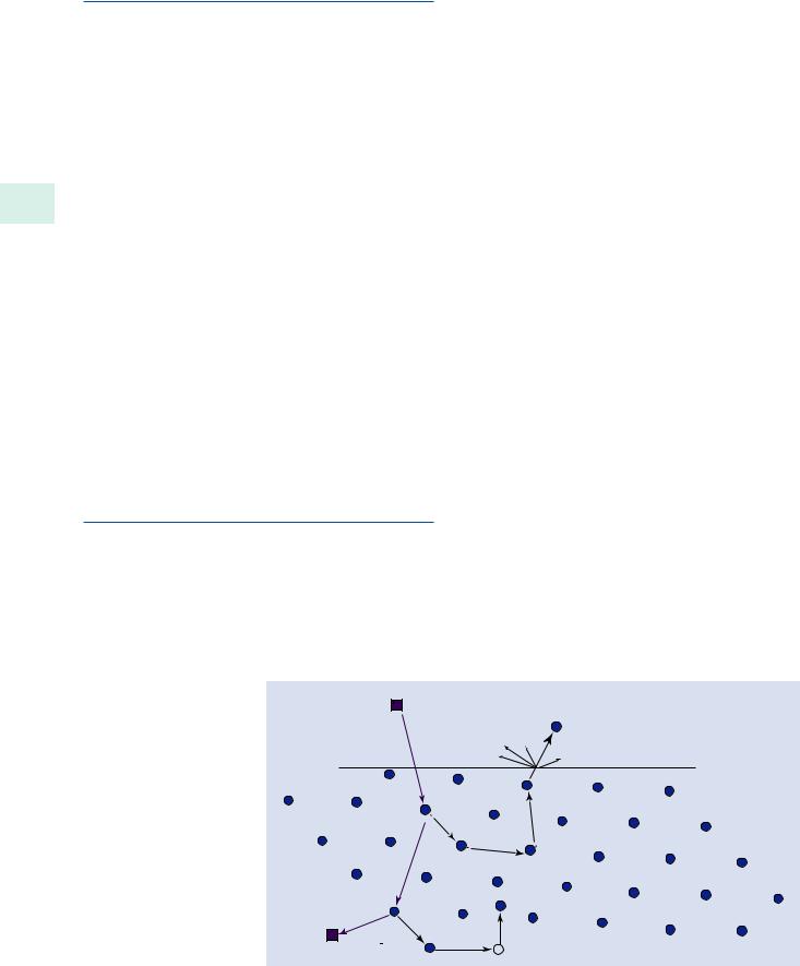
A schematic diagram of the interactions is shown in
. Fig. 30.1. Here an energetic ion is injected into a crystalline sample. The ion enters the sample at position 1. The ion is then deflected by interactions with the atomic nuclei and the electron charges. As the ion moves through the sample it has sufficient energy to knock other atoms off their respective lattice positions as shown at position 2. The target atoms that are knocked off their atomic positions can have enough energy to knock other target atoms off their atomic positions as shown at position 3. Some of the atoms that have been knocked from their atomic positions may reoccupy a lattice position or may end up in interstitial sites. There can also be lattice sites that are not reoccupied by target atoms and are left as vacancies. Both interstitials and vacancies are considered damage to the crystalline structure of the sample as shown in position 4. Most of the time, the original beam ion will end up coming to rest within the sample. This is termed ion implantation and is shown at position 5. Ion implantation results in the detection of the ion beam species in the sample. Many of the collision cascades will eventually reach the surface of the sample. Sufficient energy may be imparted to knock an atom from the surface into the vacuum. This process is called sputtering and results in a net loss of material from the sample as shown in position 6. At the same time when the ion is either entering or leaving the sample, secondary electrons are generated that are useful for producing images of the sample surface scanned by the ion beam. It is important to remember that scanning an energetic ion beam over the surface of the sample will always result in some damage to the sample. Understanding the interaction of ions
. Fig. 30.1 Schematic of some of the important ion–solid interactions that can occur
Incident |
|
|
|
primary Ga |
Secondary |
|
6 Sputtered |
|
electrons |
|
species |
|
|
e |
e |
|
|
|
|
1 |
e |
|
e |
|
|
|
Sample |
|
|
|
surface |
|
2 |
|
|
|
3 |
|
|
|
Collision |
|
|
|
cascade |
|
|
|
4 |
5 |
Interstitial |
|
|
Implanted Ga |
atom |