

- •Preface
- •Imaging Microscopic Features
- •Measuring the Crystal Structure
- •References
- •Contents
- •1.4 Simulating the Effects of Elastic Scattering: Monte Carlo Calculations
- •What Are the Main Features of the Beam Electron Interaction Volume?
- •How Does the Interaction Volume Change with Composition?
- •How Does the Interaction Volume Change with Incident Beam Energy?
- •How Does the Interaction Volume Change with Specimen Tilt?
- •1.5 A Range Equation To Estimate the Size of the Interaction Volume
- •References
- •2: Backscattered Electrons
- •2.1 Origin
- •2.2.1 BSE Response to Specimen Composition (η vs. Atomic Number, Z)
- •SEM Image Contrast with BSE: “Atomic Number Contrast”
- •SEM Image Contrast: “BSE Topographic Contrast—Number Effects”
- •2.2.3 Angular Distribution of Backscattering
- •Beam Incident at an Acute Angle to the Specimen Surface (Specimen Tilt > 0°)
- •SEM Image Contrast: “BSE Topographic Contrast—Trajectory Effects”
- •2.2.4 Spatial Distribution of Backscattering
- •Depth Distribution of Backscattering
- •Radial Distribution of Backscattered Electrons
- •2.3 Summary
- •References
- •3: Secondary Electrons
- •3.1 Origin
- •3.2 Energy Distribution
- •3.3 Escape Depth of Secondary Electrons
- •3.8 Spatial Characteristics of Secondary Electrons
- •References
- •4: X-Rays
- •4.1 Overview
- •4.2 Characteristic X-Rays
- •4.2.1 Origin
- •4.2.2 Fluorescence Yield
- •4.2.3 X-Ray Families
- •4.2.4 X-Ray Nomenclature
- •4.2.6 Characteristic X-Ray Intensity
- •Isolated Atoms
- •X-Ray Production in Thin Foils
- •X-Ray Intensity Emitted from Thick, Solid Specimens
- •4.3 X-Ray Continuum (bremsstrahlung)
- •4.3.1 X-Ray Continuum Intensity
- •4.3.3 Range of X-ray Production
- •4.4 X-Ray Absorption
- •4.5 X-Ray Fluorescence
- •References
- •5.1 Electron Beam Parameters
- •5.2 Electron Optical Parameters
- •5.2.1 Beam Energy
- •Landing Energy
- •5.2.2 Beam Diameter
- •5.2.3 Beam Current
- •5.2.4 Beam Current Density
- •5.2.5 Beam Convergence Angle, α
- •5.2.6 Beam Solid Angle
- •5.2.7 Electron Optical Brightness, β
- •Brightness Equation
- •5.2.8 Focus
- •Astigmatism
- •5.3 SEM Imaging Modes
- •5.3.1 High Depth-of-Field Mode
- •5.3.2 High-Current Mode
- •5.3.3 Resolution Mode
- •5.3.4 Low-Voltage Mode
- •5.4 Electron Detectors
- •5.4.1 Important Properties of BSE and SE for Detector Design and Operation
- •Abundance
- •Angular Distribution
- •Kinetic Energy Response
- •5.4.2 Detector Characteristics
- •Angular Measures for Electron Detectors
- •Elevation (Take-Off) Angle, ψ, and Azimuthal Angle, ζ
- •Solid Angle, Ω
- •Energy Response
- •Bandwidth
- •5.4.3 Common Types of Electron Detectors
- •Backscattered Electrons
- •Passive Detectors
- •Scintillation Detectors
- •Semiconductor BSE Detectors
- •5.4.4 Secondary Electron Detectors
- •Everhart–Thornley Detector
- •Through-the-Lens (TTL) Electron Detectors
- •TTL SE Detector
- •TTL BSE Detector
- •Measuring the DQE: BSE Semiconductor Detector
- •References
- •6: Image Formation
- •6.1 Image Construction by Scanning Action
- •6.2 Magnification
- •6.3 Making Dimensional Measurements With the SEM: How Big Is That Feature?
- •Using a Calibrated Structure in ImageJ-Fiji
- •6.4 Image Defects
- •6.4.1 Projection Distortion (Foreshortening)
- •6.4.2 Image Defocusing (Blurring)
- •6.5 Making Measurements on Surfaces With Arbitrary Topography: Stereomicroscopy
- •6.5.1 Qualitative Stereomicroscopy
- •Fixed beam, Specimen Position Altered
- •Fixed Specimen, Beam Incidence Angle Changed
- •6.5.2 Quantitative Stereomicroscopy
- •Measuring a Simple Vertical Displacement
- •References
- •7: SEM Image Interpretation
- •7.1 Information in SEM Images
- •7.2.2 Calculating Atomic Number Contrast
- •Establishing a Robust Light-Optical Analogy
- •Getting It Wrong: Breaking the Light-Optical Analogy of the Everhart–Thornley (Positive Bias) Detector
- •Deconstructing the SEM/E–T Image of Topography
- •SUM Mode (A + B)
- •DIFFERENCE Mode (A−B)
- •References
- •References
- •9: Image Defects
- •9.1 Charging
- •9.1.1 What Is Specimen Charging?
- •9.1.3 Techniques to Control Charging Artifacts (High Vacuum Instruments)
- •Observing Uncoated Specimens
- •Coating an Insulating Specimen for Charge Dissipation
- •Choosing the Coating for Imaging Morphology
- •9.2 Radiation Damage
- •9.3 Contamination
- •References
- •10: High Resolution Imaging
- •10.2 Instrumentation Considerations
- •10.4.1 SE Range Effects Produce Bright Edges (Isolated Edges)
- •10.4.4 Too Much of a Good Thing: The Bright Edge Effect Hinders Locating the True Position of an Edge for Critical Dimension Metrology
- •10.5.1 Beam Energy Strategies
- •Low Beam Energy Strategy
- •High Beam Energy Strategy
- •Making More SE1: Apply a Thin High-δ Metal Coating
- •Making Fewer BSEs, SE2, and SE3 by Eliminating Bulk Scattering From the Substrate
- •10.6 Factors That Hinder Achieving High Resolution
- •10.6.2 Pathological Specimen Behavior
- •Contamination
- •Instabilities
- •References
- •11: Low Beam Energy SEM
- •11.3 Selecting the Beam Energy to Control the Spatial Sampling of Imaging Signals
- •11.3.1 Low Beam Energy for High Lateral Resolution SEM
- •11.3.2 Low Beam Energy for High Depth Resolution SEM
- •11.3.3 Extremely Low Beam Energy Imaging
- •References
- •12.1.1 Stable Electron Source Operation
- •12.1.2 Maintaining Beam Integrity
- •12.1.4 Minimizing Contamination
- •12.3.1 Control of Specimen Charging
- •12.5 VPSEM Image Resolution
- •References
- •13: ImageJ and Fiji
- •13.1 The ImageJ Universe
- •13.2 Fiji
- •13.3 Plugins
- •13.4 Where to Learn More
- •References
- •14: SEM Imaging Checklist
- •14.1.1 Conducting or Semiconducting Specimens
- •14.1.2 Insulating Specimens
- •14.2 Electron Signals Available
- •14.2.1 Beam Electron Range
- •14.2.2 Backscattered Electrons
- •14.2.3 Secondary Electrons
- •14.3 Selecting the Electron Detector
- •14.3.2 Backscattered Electron Detectors
- •14.3.3 “Through-the-Lens” Detectors
- •14.4 Selecting the Beam Energy for SEM Imaging
- •14.4.4 High Resolution SEM Imaging
- •Strategy 1
- •Strategy 2
- •14.5 Selecting the Beam Current
- •14.5.1 High Resolution Imaging
- •14.5.2 Low Contrast Features Require High Beam Current and/or Long Frame Time to Establish Visibility
- •14.6 Image Presentation
- •14.6.1 “Live” Display Adjustments
- •14.6.2 Post-Collection Processing
- •14.7 Image Interpretation
- •14.7.1 Observer’s Point of View
- •14.7.3 Contrast Encoding
- •14.8.1 VPSEM Advantages
- •14.8.2 VPSEM Disadvantages
- •15: SEM Case Studies
- •15.1 Case Study: How High Is That Feature Relative to Another?
- •15.2 Revealing Shallow Surface Relief
- •16.1.2 Minor Artifacts: The Si-Escape Peak
- •16.1.3 Minor Artifacts: Coincidence Peaks
- •16.1.4 Minor Artifacts: Si Absorption Edge and Si Internal Fluorescence Peak
- •16.2 “Best Practices” for Electron-Excited EDS Operation
- •16.2.1 Operation of the EDS System
- •Choosing the EDS Time Constant (Resolution and Throughput)
- •Choosing the Solid Angle of the EDS
- •Selecting a Beam Current for an Acceptable Level of System Dead-Time
- •16.3.1 Detector Geometry
- •16.3.2 Process Time
- •16.3.3 Optimal Working Distance
- •16.3.4 Detector Orientation
- •16.3.5 Count Rate Linearity
- •16.3.6 Energy Calibration Linearity
- •16.3.7 Other Items
- •16.3.8 Setting Up a Quality Control Program
- •Using the QC Tools Within DTSA-II
- •Creating a QC Project
- •Linearity of Output Count Rate with Live-Time Dose
- •Resolution and Peak Position Stability with Count Rate
- •Solid Angle for Low X-ray Flux
- •Maximizing Throughput at Moderate Resolution
- •References
- •17: DTSA-II EDS Software
- •17.1 Getting Started With NIST DTSA-II
- •17.1.1 Motivation
- •17.1.2 Platform
- •17.1.3 Overview
- •17.1.4 Design
- •Simulation
- •Quantification
- •Experiment Design
- •Modeled Detectors (. Fig. 17.1)
- •Window Type (. Fig. 17.2)
- •The Optimal Working Distance (. Figs. 17.3 and 17.4)
- •Elevation Angle
- •Sample-to-Detector Distance
- •Detector Area
- •Crystal Thickness
- •Number of Channels, Energy Scale, and Zero Offset
- •Resolution at Mn Kα (Approximate)
- •Azimuthal Angle
- •Gold Layer, Aluminum Layer, Nickel Layer
- •Dead Layer
- •Zero Strobe Discriminator (. Figs. 17.7 and 17.8)
- •Material Editor Dialog (. Figs. 17.9, 17.10, 17.11, 17.12, 17.13, and 17.14)
- •17.2.1 Introduction
- •17.2.2 Monte Carlo Simulation
- •17.2.4 Optional Tables
- •References
- •18: Qualitative Elemental Analysis by Energy Dispersive X-Ray Spectrometry
- •18.1 Quality Assurance Issues for Qualitative Analysis: EDS Calibration
- •18.2 Principles of Qualitative EDS Analysis
- •Exciting Characteristic X-Rays
- •Fluorescence Yield
- •X-ray Absorption
- •Si Escape Peak
- •Coincidence Peaks
- •18.3 Performing Manual Qualitative Analysis
- •Beam Energy
- •Choosing the EDS Resolution (Detector Time Constant)
- •Obtaining Adequate Counts
- •18.4.1 Employ the Available Software Tools
- •18.4.3 Lower Photon Energy Region
- •18.4.5 Checking Your Work
- •18.5 A Worked Example of Manual Peak Identification
- •References
- •19.1 What Is a k-ratio?
- •19.3 Sets of k-ratios
- •19.5 The Analytical Total
- •19.6 Normalization
- •19.7.1 Oxygen by Assumed Stoichiometry
- •19.7.3 Element by Difference
- •19.8 Ways of Reporting Composition
- •19.8.1 Mass Fraction
- •19.8.2 Atomic Fraction
- •19.8.3 Stoichiometry
- •19.8.4 Oxide Fractions
- •Example Calculations
- •19.9 The Accuracy of Quantitative Electron-Excited X-ray Microanalysis
- •19.9.1 Standards-Based k-ratio Protocol
- •19.9.2 “Standardless Analysis”
- •19.10 Appendix
- •19.10.1 The Need for Matrix Corrections To Achieve Quantitative Analysis
- •19.10.2 The Physical Origin of Matrix Effects
- •19.10.3 ZAF Factors in Microanalysis
- •X-ray Generation With Depth, φ(ρz)
- •X-ray Absorption Effect, A
- •X-ray Fluorescence, F
- •References
- •20.2 Instrumentation Requirements
- •20.2.1 Choosing the EDS Parameters
- •EDS Spectrum Channel Energy Width and Spectrum Energy Span
- •EDS Time Constant (Resolution and Throughput)
- •EDS Calibration
- •EDS Solid Angle
- •20.2.2 Choosing the Beam Energy, E0
- •20.2.3 Measuring the Beam Current
- •20.2.4 Choosing the Beam Current
- •Optimizing Analysis Strategy
- •20.3.4 Ba-Ti Interference in BaTiSi3O9
- •20.4 The Need for an Iterative Qualitative and Quantitative Analysis Strategy
- •20.4.2 Analysis of a Stainless Steel
- •20.5 Is the Specimen Homogeneous?
- •20.6 Beam-Sensitive Specimens
- •20.6.1 Alkali Element Migration
- •20.6.2 Materials Subject to Mass Loss During Electron Bombardment—the Marshall-Hall Method
- •Thin Section Analysis
- •Bulk Biological and Organic Specimens
- •References
- •21: Trace Analysis by SEM/EDS
- •21.1 Limits of Detection for SEM/EDS Microanalysis
- •21.2.1 Estimating CDL from a Trace or Minor Constituent from Measuring a Known Standard
- •21.2.2 Estimating CDL After Determination of a Minor or Trace Constituent with Severe Peak Interference from a Major Constituent
- •21.3 Measurements of Trace Constituents by Electron-Excited Energy Dispersive X-ray Spectrometry
- •The Inevitable Physics of Remote Excitation Within the Specimen: Secondary Fluorescence Beyond the Electron Interaction Volume
- •Simulation of Long-Range Secondary X-ray Fluorescence
- •NIST DTSA II Simulation: Vertical Interface Between Two Regions of Different Composition in a Flat Bulk Target
- •NIST DTSA II Simulation: Cubic Particle Embedded in a Bulk Matrix
- •21.5 Summary
- •References
- •22.1.2 Low Beam Energy Analysis Range
- •22.2 Advantage of Low Beam Energy X-Ray Microanalysis
- •22.2.1 Improved Spatial Resolution
- •22.3 Challenges and Limitations of Low Beam Energy X-Ray Microanalysis
- •22.3.1 Reduced Access to Elements
- •22.3.3 At Low Beam Energy, Almost Everything Is Found To Be Layered
- •Analysis of Surface Contamination
- •References
- •23: Analysis of Specimens with Special Geometry: Irregular Bulk Objects and Particles
- •23.2.1 No Chemical Etching
- •23.3 Consequences of Attempting Analysis of Bulk Materials With Rough Surfaces
- •23.4.1 The Raw Analytical Total
- •23.4.2 The Shape of the EDS Spectrum
- •23.5 Best Practices for Analysis of Rough Bulk Samples
- •23.6 Particle Analysis
- •Particle Sample Preparation: Bulk Substrate
- •The Importance of Beam Placement
- •Overscanning
- •“Particle Mass Effect”
- •“Particle Absorption Effect”
- •The Analytical Total Reveals the Impact of Particle Effects
- •Does Overscanning Help?
- •23.6.6 Peak-to-Background (P/B) Method
- •Specimen Geometry Severely Affects the k-ratio, but Not the P/B
- •Using the P/B Correspondence
- •23.7 Summary
- •References
- •24: Compositional Mapping
- •24.2 X-Ray Spectrum Imaging
- •24.2.1 Utilizing XSI Datacubes
- •24.2.2 Derived Spectra
- •SUM Spectrum
- •MAXIMUM PIXEL Spectrum
- •24.3 Quantitative Compositional Mapping
- •24.4 Strategy for XSI Elemental Mapping Data Collection
- •24.4.1 Choosing the EDS Dead-Time
- •24.4.2 Choosing the Pixel Density
- •24.4.3 Choosing the Pixel Dwell Time
- •“Flash Mapping”
- •High Count Mapping
- •References
- •25.1 Gas Scattering Effects in the VPSEM
- •25.1.1 Why Doesn’t the EDS Collimator Exclude the Remote Skirt X-Rays?
- •25.2 What Can Be Done To Minimize gas Scattering in VPSEM?
- •25.2.2 Favorable Sample Characteristics
- •Particle Analysis
- •25.2.3 Unfavorable Sample Characteristics
- •References
- •26.1 Instrumentation
- •26.1.2 EDS Detector
- •26.1.3 Probe Current Measurement Device
- •Direct Measurement: Using a Faraday Cup and Picoammeter
- •A Faraday Cup
- •Electrically Isolated Stage
- •Indirect Measurement: Using a Calibration Spectrum
- •26.1.4 Conductive Coating
- •26.2 Sample Preparation
- •26.2.1 Standard Materials
- •26.2.2 Peak Reference Materials
- •26.3 Initial Set-Up
- •26.3.1 Calibrating the EDS Detector
- •Selecting a Pulse Process Time Constant
- •Energy Calibration
- •Quality Control
- •Sample Orientation
- •Detector Position
- •Probe Current
- •26.4 Collecting Data
- •26.4.1 Exploratory Spectrum
- •26.4.2 Experiment Optimization
- •26.4.3 Selecting Standards
- •26.4.4 Reference Spectra
- •26.4.5 Collecting Standards
- •26.4.6 Collecting Peak-Fitting References
- •26.5 Data Analysis
- •26.5.2 Quantification
- •26.6 Quality Check
- •Reference
- •27.2 Case Study: Aluminum Wire Failures in Residential Wiring
- •References
- •28: Cathodoluminescence
- •28.1 Origin
- •28.2 Measuring Cathodoluminescence
- •28.3 Applications of CL
- •28.3.1 Geology
- •Carbonado Diamond
- •Ancient Impact Zircons
- •28.3.2 Materials Science
- •Semiconductors
- •Lead-Acid Battery Plate Reactions
- •28.3.3 Organic Compounds
- •References
- •29.1.1 Single Crystals
- •29.1.2 Polycrystalline Materials
- •29.1.3 Conditions for Detecting Electron Channeling Contrast
- •Specimen Preparation
- •Instrument Conditions
- •29.2.1 Origin of EBSD Patterns
- •29.2.2 Cameras for EBSD Pattern Detection
- •29.2.3 EBSD Spatial Resolution
- •29.2.5 Steps in Typical EBSD Measurements
- •Sample Preparation for EBSD
- •Align Sample in the SEM
- •Check for EBSD Patterns
- •Adjust SEM and Select EBSD Map Parameters
- •Run the Automated Map
- •29.2.6 Display of the Acquired Data
- •29.2.7 Other Map Components
- •29.2.10 Application Example
- •Application of EBSD To Understand Meteorite Formation
- •29.2.11 Summary
- •Specimen Considerations
- •EBSD Detector
- •Selection of Candidate Crystallographic Phases
- •Microscope Operating Conditions and Pattern Optimization
- •Selection of EBSD Acquisition Parameters
- •Collect the Orientation Map
- •References
- •30.1 Introduction
- •30.2 Ion–Solid Interactions
- •30.3 Focused Ion Beam Systems
- •30.5 Preparation of Samples for SEM
- •30.5.1 Cross-Section Preparation
- •30.5.2 FIB Sample Preparation for 3D Techniques and Imaging
- •30.6 Summary
- •References
- •31: Ion Beam Microscopy
- •31.1 What Is So Useful About Ions?
- •31.2 Generating Ion Beams
- •31.3 Signal Generation in the HIM
- •31.5 Patterning with Ion Beams
- •31.7 Chemical Microanalysis with Ion Beams
- •References
- •Appendix
- •A Database of Electron–Solid Interactions
- •A Database of Electron–Solid Interactions
- •Introduction
- •Backscattered Electrons
- •Secondary Yields
- •Stopping Powers
- •X-ray Ionization Cross Sections
- •Conclusions
- •References
- •Index
- •Reference List
- •Index
\134 Chapter 9 · Image Defects
SEM images are subject to defects that can arise from a variety of mechanisms, including charging, radiation damage, contamination, and moiré fringe effects, among others. Image defects are very dependent on the specific nature of the specimen, and often they are anecdotal, experienced but not reported in the SEM literature. The examples described below are not a complete catalog but are presented to alert the microscopist to the possibility of such image defects so as to avoid interpreting artifact as fact.
Faraday cage of EDS Everhart -Thornley
detector
Bore of  objective lens
9.1\ Charging
Charging is one of the major image defects commonly encountered in SEM imaging, especially when using the Everhart–Thornley (positive bias) “secondary electron” detector, which is especially sensitive to even slight charging.
Annular
BSE detector
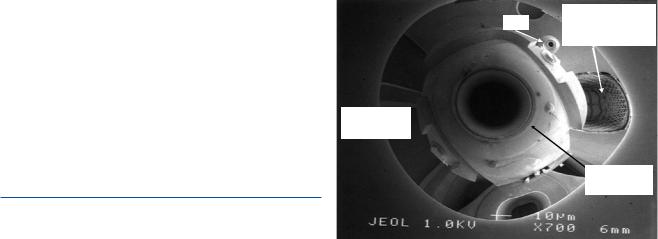
. Fig. 9.1 SEM image (Everhart–Thornley detector, positive bias) obtained by disconnecting grounding wire from the specimen stage and reflecting the scan from a flat, conducting substrate; E0 = 1 keV
9 |
9.1.1\ What Is Specimen Charging? |
|
|
|
|
|
|
|
The specimen can be thought of as an electrical junction into |
||
|
|||
|
which the beam current, iB, flows. The phenomena of back- |
||
|
scattering of the beam electrons and secondary electron |
||
|
emission represent currents flowing out of the junction, iBSE |
||
|
(= η iB) and iSE (= δ iB). For a copper target and an incident |
||
|
beam energy of 20 keV, η is approximately 0.3 and δ is |
||
|
approximately 0.1, which together account for 0.4 or 40 % of |
||
|
the charges injected into the specimen by the beam current. |
||
|
The remaining beam current must flow from the specimen to |
||
|
ground to avoid the accumulation of charge in the junction |
||
|
(Kirchoff’s current law). The balance of the currents for a |
||
|
non-charging junction is then given by |
|
|
|
|
∑iin = ∑iout |
|
|
|
iB = iBSE + iSE + iSC \ |
(9.1) |
|
where iSC is the specimen (or absorbed) current. For the |
||
|
|
example of copper, iSC = 0.6 iB. |
|
|
|
The specimen stage is typically constructed so that the |
|
|
|
specimen is electrically isolated from electrical ground to |
|
|
|
permit various measurements. A wire connection to the |
|
|
|
stage establishes the conduction path for the specimen cur- |
|
|
|
rent to travel to the electrical ground. This design enables a |
|
|
|
current meter to be installed in this path to ground, allowing |
|
|
|
direct measurement of the specimen current and enabling |
|
|
|
measurement of the true beam current with a Faraday cup |
|
|
|
(which captures all electrons that enter it) in place of the |
|
|
|
specimen. Moreover, this specimen current signal can be |
|
|
|
used to form an image of the specimen (see the “Electron |
|
|
|
Detectors” module) However, if the electrical path from the |
|
|
|
specimen surface to ground is interrupted, the conditions for |
|
|
|
charge balance in Eq. (9.1) cannot be established, even if the |
|
|
specimen is a metallic conductor. The electrons injected into |
||
|
the specimen by the beam will then accumulate, and the |
||
|
specimen will develop a high negative electrical |
charge |
|
relative to ground. The electrical field from this negative charge will decelerate the incoming beam electrons, and in extreme cases the specimen will actually act like an electron mirror. The scanning beam will be reflected before reaching the surface, so that it actually scans the inside of the specimen chamber, creating an image that reveals the objective lens, detectors, and other features of the specimen chamber, as shown in . Fig. 9.1.
If the electrical path to ground is established, then the excess charges will be dissipated in the form of the specimen current provided the specimen has sufficient conductivity. Because all materials (except superconductors) have the property of electrical resistivity, ρ, the specimen has a resistance R (R = ρ L/A, where L is the length of the specimen and A is the cross section), and the passage of the specimen current, iSC, through this resistance will cause a potential drop across the specimen, V = iSC R. For a metal, ρ is typically of the order of 10−6 Ω-cm, so that a specimen 1-cm thick with a cross-sectional area of 1 cm2 will have a resistance of 10−6 Ω, and a beam current of 1 nA (10−9 A) will cause a potential of about 10−15 V to develop across the specimen. For a high purity (undoped) semiconductor such as silicon or germanium, ρ is approximately 104 to 106 Ω-cm, and the 1-nA beam will cause a potential of 1 mV (10−3 V) or less to develop across the 1-cm cube specimen, which is still negligible. The flow of the specimen current to ground becomes a critical problem when dealing with non-conducting (insulating) specimens. Insulating specimens include a very wide variety of materials such as plastics, polymers, elastomers, minerals, rocks, glasses, ceramics, and others, which may be encountered as bulk solids, porous solids, foams, particles, or fibers. Virtually all biological specimens become non-con- ducting when water is removed by drying, substitution with low vapor pressure polymers, or frozen in place. For an insulator such as an oxide, ρ is very high, 106 to 1016 Ω-cm, which prevents the smooth motion of the electrons injected by the beam through the specimen to ground; electrons accumulate
9.1 · Charging
in the immediate vicinity of the beam impact, raising the local potential and creating a range of phenomena described as “charging.”
9.1.2\ Recognizing Charging Phenomena
in SEM Images
Charging phenomena cover a wide range of observed behaviors in SEM images of imperfectly conducting specimens. Secondary electrons (SEs) are emitted with very low energy, by definition ESE < 50 eV, with most carrying less than 5 eV. Such low energy, slow-moving SEs can be strongly deflected by local electrical fields caused by charging. The Everhart–Thornley (positive bias) detector collects SEs by means of a positive potential of a few hundred volts (e.g., +300 V) applied to the Faraday cage at a distance of several centimeters (e.g., 3 cm) from the specimen, creating an electrical field at the specimen of approximately 104 V/m. SEs emitted from a conducting specimen are strongly attracted to follow the field lines from the grounded specimen surface to the positively biased Faraday cage grid, and thus into the high voltage field applied to the face of the scintillator of the Everhart–Thornley (E–T) detector. If the specimen charges locally to develop even a few volts’ potential, the local electrical field from the charged region relative to nearby uncharged areas of the specimen a few micrometers away or to the grounded stub a few millimeters away is likely to be much stronger (105 to 107 V/m) than the field imposed by the E–T detector. Depending on the positive or negative character, this specimen field may have either a repulsive or an attractive effect. Thus, depending on the details of the local electrical field, the collection of SEs by the E–T detector may be enhanced or diminished. Negatively charging areas will appear bright, while in positively charging areas the SEs are attracted back to the specimen surface or to the stub so that such a region appears dark. Thus, the typical
135 |
|
9 |
|
|
|
appearance of an isolated insulating particle undergoing charging on a conducting surface is a bright, often saturated signal (possibly accompanied by amplifier overloading effects due to signal saturation) surrounded by a dark halo that extends over surrounding conducting portions of the specimen where the local field induced by the charging causes the SEs to be recollected. This type of voltage contrast must be regarded as an artifact, because it interferes with and overwhelms the regular behavior of secondary electron (SE) emission with local surface inclination that we depend upon for sensible image interpretation of specimen topography with the E–T detector. . Figure 9.2 shows examples of charging effects observed when imaging insulating particles on a conducting metallic substrate with the E–T (positive bias) detector. There are regions on the particles that are extremely bright due to high negative charging that increases the detector collection efficiency surrounded by a dark
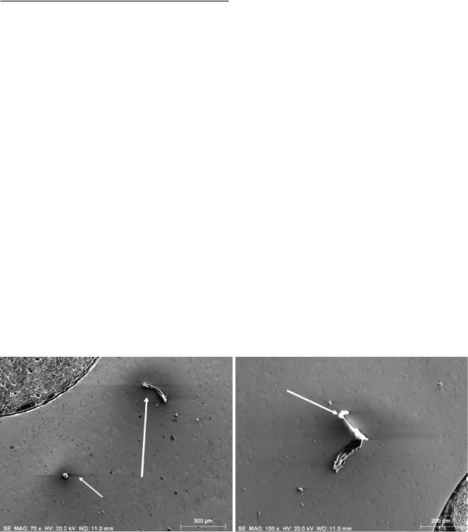
“halo” where a positive mirror charge develops, lowering the collection efficiency. Often these charging effects, while extreme in the E–T (positive bias) image due to the disruption of SE trajectories, will be negligible in a backscattered electron (BSE) image simultaneously collected from the same field of view, because the much higher energy BSEs are not significantly deflected by the low surface potential. An example is shown in . Fig. 9.3, where the SE image,
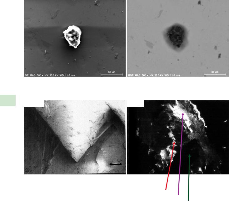
. Fig. 9.3a, shows extreme bright-dark regions due to charging while the corresponding BSE image, . Fig. 9.3b, shows details of the structure of the particle. In more extreme cases of charging, the true topographic contrast image of the specimen may be completely overwhelmed by the charging effects, which in the most extreme cases will actually deflect the beam causing image discontinuities. An example is shown in . Fig. 9.4, which compares images (Everhart– Thornley detector, positive bias) of an uncoated calcite crystal at E0 = 1.5 keV, where the true shape of the object can be seen, and at E0 = 5 keV, where charging completely overwhelms the topographic contrast.
Extremely bright regions:
Increased SE emission/collection
 Dark halo:
decreased SE collection
. Fig. 9.2 Examples of charging artifacts observed in images of dust particles on a metallic substrate. E0 = 20 keV; Everhart–Thornley (positive bias) detector
136\ Chapter 9 · Image Defects
SE |
BSE |
. Fig. 9.3 Comparison of images of a dust particle on a metallic substrate: (left) Everhart–Thornley (positive bias) detector; (right) semiconductor BSE (sum) detector; E0 = 20 keV
9 |
E0 |
= 1.5 keV |
E0 = 5 keV |
|
100 µm
Extreme charging:
1. Scan deflection
2. Fully saturated areas (gray level 255)
3. Completely dark areas (gray level 0)
. Fig. 9.4 Comparison of images of an uncoated calcite crystal viewed at (left) E0 = 1.5 keV, showing topographic contrast; (right) E0 = 5 keV, showing extreme charging effects; Everhart–Thornley (positive bias) detector
Charging phenomena are incompletely understood and are often found to be dynamic with time, a result of the time- dependent motion of the beam due to scanning action and due to the electrical breakdown properties of materials as well as differences in surface and bulk resistivity. An insulating specimen acts as a local capacitor, so that placing the beam at a pixel causes a charge to build up with an RC time constant as a function of the dwell time, followed by a decay of that charge when the beam moves away. Depending on the exact material properties, especially the surface resistivity which is often much lower than the bulk resistivity, and the
beam conditions (beam energy, current, and scan rate), the injected charge may only partially dissipate before the beam returns in the scan cycle, leading to strong effects in SEM images. Moreover, local specimen properties may cause charging effects to vary with position in the same image. A time-dependent charging situation at a pixel is shown schematically in . Fig. 9.5, where the surface potential at a particular pixel accumulates with the dwell time and then decays until the beam returns. In more extreme behavior, the accumulated charge may cause local electrical breakdown and abruptly discharge to ground. The time dependence of
9.1 · Charging
–V
0
0 |
Time |
. Fig. 9.5 Schematic illustration of the potential developed at a pixel as a function of time showing repeated beam dwells
charging can result in very different imaging results as the pixel dwell time is changed from rapid scanning for surveying a specimen to slow scanning for recording images with better signal-to-noise. An example of this phenomenon is
137 |
|
9 |
|
|
|
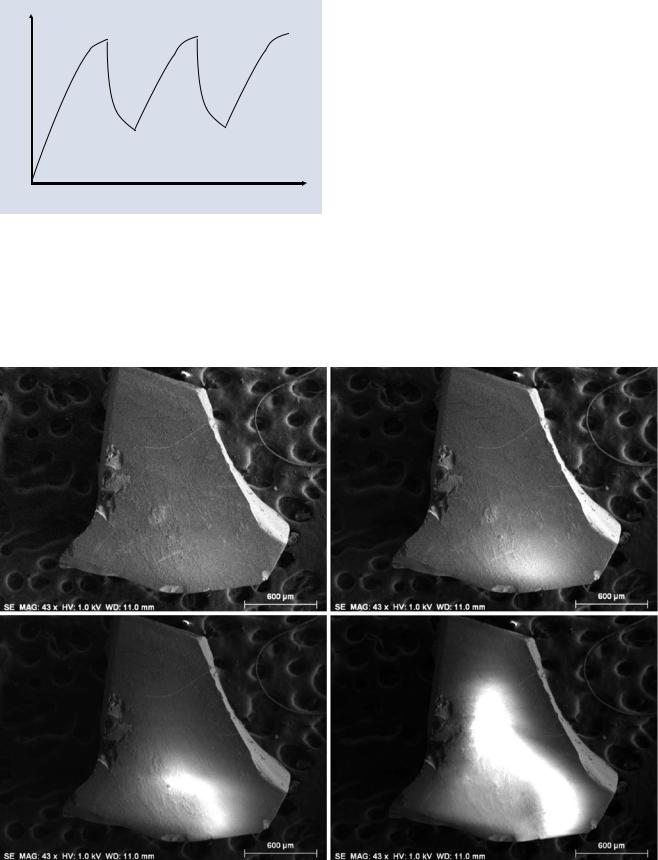
shown in . Fig. 9.6, where an image of an uncoated mineral fragment taken with E0 = 1 keV appears to be free of charging artifacts with a pixel dwell time of 1.6 μs, but longer dwell times lead to the in-growth of a bright region due to charging. Charging artifacts can often be minimized by avoiding slow scanning through the use of rapid scanning and summing repeated scans to improve the signal-to-noise of the final image.
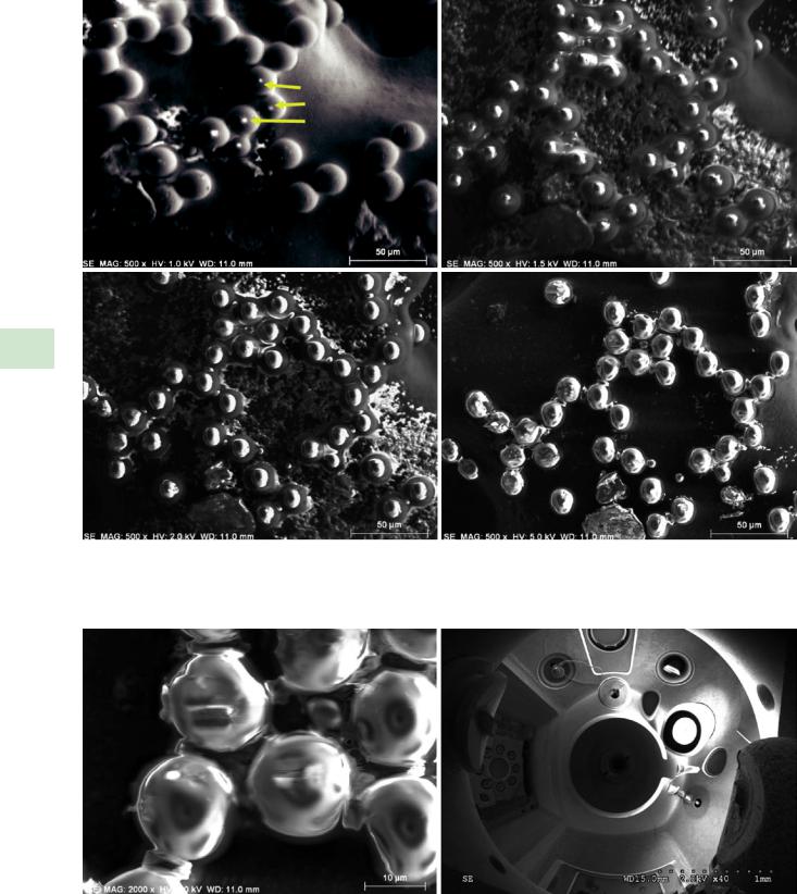
Charging of some specimens can create contrast that can easily be misinterpreted as specimen features. An example is shown in . Fig. 9.7, where most of the polystyrene latex spheres (PSLs) imaged at E0 = 1 keV with the Everhart– Thornley (positive bias) detector show true topographic details, but five of the PSLs have bright dots at the center, which might easily be mistaken for high atomic number inclusions or fine scale topographic features rising above the spherical surfaces. Raising the beam energy to 1.5 keV and higher reveals progressively more extensive and obvious evidence of charging artifacts. The nature of this charging artifact is revealed in . Fig. 9.8, which compares an image of the PSLs at higher magnification and E0 = 5 keV with a low
1.6 µs |
4 µs |
8 µs |
32 µs |
. Fig. 9.6 Sequence of images of an uncoated quartz fragment imaged at E0 = 1 keV with increasing pixel dwell times, showing development of charging; Everhart–Thornley (positive bias) detector
\138 Chapter 9 · Image Defects
1 keV |
|
1.5 keV |
|
|
|
 Incipient
 Charging
 Artifacts
2 keV |
|
5 keV |
|
|
|
9
. Fig. 9.7 Polystyrene latex spheres imaged over a range of beam energy, showing development of charging artifacts; Everhart–Thornley (positive bias) detector
5 keV |
|
2 keV |
|
|
|
. Fig. 9.8 (left) Higher magnification image of PSLs at E0 = 5 keV; (right) reflection image from large plastic sphere that was charged at E0 = 10 keV and then imaged at E0 = 2 keV; Everhart–Thornley (positive bias) detector