

- •Preface
- •Imaging Microscopic Features
- •Measuring the Crystal Structure
- •References
- •Contents
- •1.4 Simulating the Effects of Elastic Scattering: Monte Carlo Calculations
- •What Are the Main Features of the Beam Electron Interaction Volume?
- •How Does the Interaction Volume Change with Composition?
- •How Does the Interaction Volume Change with Incident Beam Energy?
- •How Does the Interaction Volume Change with Specimen Tilt?
- •1.5 A Range Equation To Estimate the Size of the Interaction Volume
- •References
- •2: Backscattered Electrons
- •2.1 Origin
- •2.2.1 BSE Response to Specimen Composition (η vs. Atomic Number, Z)
- •SEM Image Contrast with BSE: “Atomic Number Contrast”
- •SEM Image Contrast: “BSE Topographic Contrast—Number Effects”
- •2.2.3 Angular Distribution of Backscattering
- •Beam Incident at an Acute Angle to the Specimen Surface (Specimen Tilt > 0°)
- •SEM Image Contrast: “BSE Topographic Contrast—Trajectory Effects”
- •2.2.4 Spatial Distribution of Backscattering
- •Depth Distribution of Backscattering
- •Radial Distribution of Backscattered Electrons
- •2.3 Summary
- •References
- •3: Secondary Electrons
- •3.1 Origin
- •3.2 Energy Distribution
- •3.3 Escape Depth of Secondary Electrons
- •3.8 Spatial Characteristics of Secondary Electrons
- •References
- •4: X-Rays
- •4.1 Overview
- •4.2 Characteristic X-Rays
- •4.2.1 Origin
- •4.2.2 Fluorescence Yield
- •4.2.3 X-Ray Families
- •4.2.4 X-Ray Nomenclature
- •4.2.6 Characteristic X-Ray Intensity
- •Isolated Atoms
- •X-Ray Production in Thin Foils
- •X-Ray Intensity Emitted from Thick, Solid Specimens
- •4.3 X-Ray Continuum (bremsstrahlung)
- •4.3.1 X-Ray Continuum Intensity
- •4.3.3 Range of X-ray Production
- •4.4 X-Ray Absorption
- •4.5 X-Ray Fluorescence
- •References
- •5.1 Electron Beam Parameters
- •5.2 Electron Optical Parameters
- •5.2.1 Beam Energy
- •Landing Energy
- •5.2.2 Beam Diameter
- •5.2.3 Beam Current
- •5.2.4 Beam Current Density
- •5.2.5 Beam Convergence Angle, α
- •5.2.6 Beam Solid Angle
- •5.2.7 Electron Optical Brightness, β
- •Brightness Equation
- •5.2.8 Focus
- •Astigmatism
- •5.3 SEM Imaging Modes
- •5.3.1 High Depth-of-Field Mode
- •5.3.2 High-Current Mode
- •5.3.3 Resolution Mode
- •5.3.4 Low-Voltage Mode
- •5.4 Electron Detectors
- •5.4.1 Important Properties of BSE and SE for Detector Design and Operation
- •Abundance
- •Angular Distribution
- •Kinetic Energy Response
- •5.4.2 Detector Characteristics
- •Angular Measures for Electron Detectors
- •Elevation (Take-Off) Angle, ψ, and Azimuthal Angle, ζ
- •Solid Angle, Ω
- •Energy Response
- •Bandwidth
- •5.4.3 Common Types of Electron Detectors
- •Backscattered Electrons
- •Passive Detectors
- •Scintillation Detectors
- •Semiconductor BSE Detectors
- •5.4.4 Secondary Electron Detectors
- •Everhart–Thornley Detector
- •Through-the-Lens (TTL) Electron Detectors
- •TTL SE Detector
- •TTL BSE Detector
- •Measuring the DQE: BSE Semiconductor Detector
- •References
- •6: Image Formation
- •6.1 Image Construction by Scanning Action
- •6.2 Magnification
- •6.3 Making Dimensional Measurements With the SEM: How Big Is That Feature?
- •Using a Calibrated Structure in ImageJ-Fiji
- •6.4 Image Defects
- •6.4.1 Projection Distortion (Foreshortening)
- •6.4.2 Image Defocusing (Blurring)
- •6.5 Making Measurements on Surfaces With Arbitrary Topography: Stereomicroscopy
- •6.5.1 Qualitative Stereomicroscopy
- •Fixed beam, Specimen Position Altered
- •Fixed Specimen, Beam Incidence Angle Changed
- •6.5.2 Quantitative Stereomicroscopy
- •Measuring a Simple Vertical Displacement
- •References
- •7: SEM Image Interpretation
- •7.1 Information in SEM Images
- •7.2.2 Calculating Atomic Number Contrast
- •Establishing a Robust Light-Optical Analogy
- •Getting It Wrong: Breaking the Light-Optical Analogy of the Everhart–Thornley (Positive Bias) Detector
- •Deconstructing the SEM/E–T Image of Topography
- •SUM Mode (A + B)
- •DIFFERENCE Mode (A−B)
- •References
- •References
- •9: Image Defects
- •9.1 Charging
- •9.1.1 What Is Specimen Charging?
- •9.1.3 Techniques to Control Charging Artifacts (High Vacuum Instruments)
- •Observing Uncoated Specimens
- •Coating an Insulating Specimen for Charge Dissipation
- •Choosing the Coating for Imaging Morphology
- •9.2 Radiation Damage
- •9.3 Contamination
- •References
- •10: High Resolution Imaging
- •10.2 Instrumentation Considerations
- •10.4.1 SE Range Effects Produce Bright Edges (Isolated Edges)
- •10.4.4 Too Much of a Good Thing: The Bright Edge Effect Hinders Locating the True Position of an Edge for Critical Dimension Metrology
- •10.5.1 Beam Energy Strategies
- •Low Beam Energy Strategy
- •High Beam Energy Strategy
- •Making More SE1: Apply a Thin High-δ Metal Coating
- •Making Fewer BSEs, SE2, and SE3 by Eliminating Bulk Scattering From the Substrate
- •10.6 Factors That Hinder Achieving High Resolution
- •10.6.2 Pathological Specimen Behavior
- •Contamination
- •Instabilities
- •References
- •11: Low Beam Energy SEM
- •11.3 Selecting the Beam Energy to Control the Spatial Sampling of Imaging Signals
- •11.3.1 Low Beam Energy for High Lateral Resolution SEM
- •11.3.2 Low Beam Energy for High Depth Resolution SEM
- •11.3.3 Extremely Low Beam Energy Imaging
- •References
- •12.1.1 Stable Electron Source Operation
- •12.1.2 Maintaining Beam Integrity
- •12.1.4 Minimizing Contamination
- •12.3.1 Control of Specimen Charging
- •12.5 VPSEM Image Resolution
- •References
- •13: ImageJ and Fiji
- •13.1 The ImageJ Universe
- •13.2 Fiji
- •13.3 Plugins
- •13.4 Where to Learn More
- •References
- •14: SEM Imaging Checklist
- •14.1.1 Conducting or Semiconducting Specimens
- •14.1.2 Insulating Specimens
- •14.2 Electron Signals Available
- •14.2.1 Beam Electron Range
- •14.2.2 Backscattered Electrons
- •14.2.3 Secondary Electrons
- •14.3 Selecting the Electron Detector
- •14.3.2 Backscattered Electron Detectors
- •14.3.3 “Through-the-Lens” Detectors
- •14.4 Selecting the Beam Energy for SEM Imaging
- •14.4.4 High Resolution SEM Imaging
- •Strategy 1
- •Strategy 2
- •14.5 Selecting the Beam Current
- •14.5.1 High Resolution Imaging
- •14.5.2 Low Contrast Features Require High Beam Current and/or Long Frame Time to Establish Visibility
- •14.6 Image Presentation
- •14.6.1 “Live” Display Adjustments
- •14.6.2 Post-Collection Processing
- •14.7 Image Interpretation
- •14.7.1 Observer’s Point of View
- •14.7.3 Contrast Encoding
- •14.8.1 VPSEM Advantages
- •14.8.2 VPSEM Disadvantages
- •15: SEM Case Studies
- •15.1 Case Study: How High Is That Feature Relative to Another?
- •15.2 Revealing Shallow Surface Relief
- •16.1.2 Minor Artifacts: The Si-Escape Peak
- •16.1.3 Minor Artifacts: Coincidence Peaks
- •16.1.4 Minor Artifacts: Si Absorption Edge and Si Internal Fluorescence Peak
- •16.2 “Best Practices” for Electron-Excited EDS Operation
- •16.2.1 Operation of the EDS System
- •Choosing the EDS Time Constant (Resolution and Throughput)
- •Choosing the Solid Angle of the EDS
- •Selecting a Beam Current for an Acceptable Level of System Dead-Time
- •16.3.1 Detector Geometry
- •16.3.2 Process Time
- •16.3.3 Optimal Working Distance
- •16.3.4 Detector Orientation
- •16.3.5 Count Rate Linearity
- •16.3.6 Energy Calibration Linearity
- •16.3.7 Other Items
- •16.3.8 Setting Up a Quality Control Program
- •Using the QC Tools Within DTSA-II
- •Creating a QC Project
- •Linearity of Output Count Rate with Live-Time Dose
- •Resolution and Peak Position Stability with Count Rate
- •Solid Angle for Low X-ray Flux
- •Maximizing Throughput at Moderate Resolution
- •References
- •17: DTSA-II EDS Software
- •17.1 Getting Started With NIST DTSA-II
- •17.1.1 Motivation
- •17.1.2 Platform
- •17.1.3 Overview
- •17.1.4 Design
- •Simulation
- •Quantification
- •Experiment Design
- •Modeled Detectors (. Fig. 17.1)
- •Window Type (. Fig. 17.2)
- •The Optimal Working Distance (. Figs. 17.3 and 17.4)
- •Elevation Angle
- •Sample-to-Detector Distance
- •Detector Area
- •Crystal Thickness
- •Number of Channels, Energy Scale, and Zero Offset
- •Resolution at Mn Kα (Approximate)
- •Azimuthal Angle
- •Gold Layer, Aluminum Layer, Nickel Layer
- •Dead Layer
- •Zero Strobe Discriminator (. Figs. 17.7 and 17.8)
- •Material Editor Dialog (. Figs. 17.9, 17.10, 17.11, 17.12, 17.13, and 17.14)
- •17.2.1 Introduction
- •17.2.2 Monte Carlo Simulation
- •17.2.4 Optional Tables
- •References
- •18: Qualitative Elemental Analysis by Energy Dispersive X-Ray Spectrometry
- •18.1 Quality Assurance Issues for Qualitative Analysis: EDS Calibration
- •18.2 Principles of Qualitative EDS Analysis
- •Exciting Characteristic X-Rays
- •Fluorescence Yield
- •X-ray Absorption
- •Si Escape Peak
- •Coincidence Peaks
- •18.3 Performing Manual Qualitative Analysis
- •Beam Energy
- •Choosing the EDS Resolution (Detector Time Constant)
- •Obtaining Adequate Counts
- •18.4.1 Employ the Available Software Tools
- •18.4.3 Lower Photon Energy Region
- •18.4.5 Checking Your Work
- •18.5 A Worked Example of Manual Peak Identification
- •References
- •19.1 What Is a k-ratio?
- •19.3 Sets of k-ratios
- •19.5 The Analytical Total
- •19.6 Normalization
- •19.7.1 Oxygen by Assumed Stoichiometry
- •19.7.3 Element by Difference
- •19.8 Ways of Reporting Composition
- •19.8.1 Mass Fraction
- •19.8.2 Atomic Fraction
- •19.8.3 Stoichiometry
- •19.8.4 Oxide Fractions
- •Example Calculations
- •19.9 The Accuracy of Quantitative Electron-Excited X-ray Microanalysis
- •19.9.1 Standards-Based k-ratio Protocol
- •19.9.2 “Standardless Analysis”
- •19.10 Appendix
- •19.10.1 The Need for Matrix Corrections To Achieve Quantitative Analysis
- •19.10.2 The Physical Origin of Matrix Effects
- •19.10.3 ZAF Factors in Microanalysis
- •X-ray Generation With Depth, φ(ρz)
- •X-ray Absorption Effect, A
- •X-ray Fluorescence, F
- •References
- •20.2 Instrumentation Requirements
- •20.2.1 Choosing the EDS Parameters
- •EDS Spectrum Channel Energy Width and Spectrum Energy Span
- •EDS Time Constant (Resolution and Throughput)
- •EDS Calibration
- •EDS Solid Angle
- •20.2.2 Choosing the Beam Energy, E0
- •20.2.3 Measuring the Beam Current
- •20.2.4 Choosing the Beam Current
- •Optimizing Analysis Strategy
- •20.3.4 Ba-Ti Interference in BaTiSi3O9
- •20.4 The Need for an Iterative Qualitative and Quantitative Analysis Strategy
- •20.4.2 Analysis of a Stainless Steel
- •20.5 Is the Specimen Homogeneous?
- •20.6 Beam-Sensitive Specimens
- •20.6.1 Alkali Element Migration
- •20.6.2 Materials Subject to Mass Loss During Electron Bombardment—the Marshall-Hall Method
- •Thin Section Analysis
- •Bulk Biological and Organic Specimens
- •References
- •21: Trace Analysis by SEM/EDS
- •21.1 Limits of Detection for SEM/EDS Microanalysis
- •21.2.1 Estimating CDL from a Trace or Minor Constituent from Measuring a Known Standard
- •21.2.2 Estimating CDL After Determination of a Minor or Trace Constituent with Severe Peak Interference from a Major Constituent
- •21.3 Measurements of Trace Constituents by Electron-Excited Energy Dispersive X-ray Spectrometry
- •The Inevitable Physics of Remote Excitation Within the Specimen: Secondary Fluorescence Beyond the Electron Interaction Volume
- •Simulation of Long-Range Secondary X-ray Fluorescence
- •NIST DTSA II Simulation: Vertical Interface Between Two Regions of Different Composition in a Flat Bulk Target
- •NIST DTSA II Simulation: Cubic Particle Embedded in a Bulk Matrix
- •21.5 Summary
- •References
- •22.1.2 Low Beam Energy Analysis Range
- •22.2 Advantage of Low Beam Energy X-Ray Microanalysis
- •22.2.1 Improved Spatial Resolution
- •22.3 Challenges and Limitations of Low Beam Energy X-Ray Microanalysis
- •22.3.1 Reduced Access to Elements
- •22.3.3 At Low Beam Energy, Almost Everything Is Found To Be Layered
- •Analysis of Surface Contamination
- •References
- •23: Analysis of Specimens with Special Geometry: Irregular Bulk Objects and Particles
- •23.2.1 No Chemical Etching
- •23.3 Consequences of Attempting Analysis of Bulk Materials With Rough Surfaces
- •23.4.1 The Raw Analytical Total
- •23.4.2 The Shape of the EDS Spectrum
- •23.5 Best Practices for Analysis of Rough Bulk Samples
- •23.6 Particle Analysis
- •Particle Sample Preparation: Bulk Substrate
- •The Importance of Beam Placement
- •Overscanning
- •“Particle Mass Effect”
- •“Particle Absorption Effect”
- •The Analytical Total Reveals the Impact of Particle Effects
- •Does Overscanning Help?
- •23.6.6 Peak-to-Background (P/B) Method
- •Specimen Geometry Severely Affects the k-ratio, but Not the P/B
- •Using the P/B Correspondence
- •23.7 Summary
- •References
- •24: Compositional Mapping
- •24.2 X-Ray Spectrum Imaging
- •24.2.1 Utilizing XSI Datacubes
- •24.2.2 Derived Spectra
- •SUM Spectrum
- •MAXIMUM PIXEL Spectrum
- •24.3 Quantitative Compositional Mapping
- •24.4 Strategy for XSI Elemental Mapping Data Collection
- •24.4.1 Choosing the EDS Dead-Time
- •24.4.2 Choosing the Pixel Density
- •24.4.3 Choosing the Pixel Dwell Time
- •“Flash Mapping”
- •High Count Mapping
- •References
- •25.1 Gas Scattering Effects in the VPSEM
- •25.1.1 Why Doesn’t the EDS Collimator Exclude the Remote Skirt X-Rays?
- •25.2 What Can Be Done To Minimize gas Scattering in VPSEM?
- •25.2.2 Favorable Sample Characteristics
- •Particle Analysis
- •25.2.3 Unfavorable Sample Characteristics
- •References
- •26.1 Instrumentation
- •26.1.2 EDS Detector
- •26.1.3 Probe Current Measurement Device
- •Direct Measurement: Using a Faraday Cup and Picoammeter
- •A Faraday Cup
- •Electrically Isolated Stage
- •Indirect Measurement: Using a Calibration Spectrum
- •26.1.4 Conductive Coating
- •26.2 Sample Preparation
- •26.2.1 Standard Materials
- •26.2.2 Peak Reference Materials
- •26.3 Initial Set-Up
- •26.3.1 Calibrating the EDS Detector
- •Selecting a Pulse Process Time Constant
- •Energy Calibration
- •Quality Control
- •Sample Orientation
- •Detector Position
- •Probe Current
- •26.4 Collecting Data
- •26.4.1 Exploratory Spectrum
- •26.4.2 Experiment Optimization
- •26.4.3 Selecting Standards
- •26.4.4 Reference Spectra
- •26.4.5 Collecting Standards
- •26.4.6 Collecting Peak-Fitting References
- •26.5 Data Analysis
- •26.5.2 Quantification
- •26.6 Quality Check
- •Reference
- •27.2 Case Study: Aluminum Wire Failures in Residential Wiring
- •References
- •28: Cathodoluminescence
- •28.1 Origin
- •28.2 Measuring Cathodoluminescence
- •28.3 Applications of CL
- •28.3.1 Geology
- •Carbonado Diamond
- •Ancient Impact Zircons
- •28.3.2 Materials Science
- •Semiconductors
- •Lead-Acid Battery Plate Reactions
- •28.3.3 Organic Compounds
- •References
- •29.1.1 Single Crystals
- •29.1.2 Polycrystalline Materials
- •29.1.3 Conditions for Detecting Electron Channeling Contrast
- •Specimen Preparation
- •Instrument Conditions
- •29.2.1 Origin of EBSD Patterns
- •29.2.2 Cameras for EBSD Pattern Detection
- •29.2.3 EBSD Spatial Resolution
- •29.2.5 Steps in Typical EBSD Measurements
- •Sample Preparation for EBSD
- •Align Sample in the SEM
- •Check for EBSD Patterns
- •Adjust SEM and Select EBSD Map Parameters
- •Run the Automated Map
- •29.2.6 Display of the Acquired Data
- •29.2.7 Other Map Components
- •29.2.10 Application Example
- •Application of EBSD To Understand Meteorite Formation
- •29.2.11 Summary
- •Specimen Considerations
- •EBSD Detector
- •Selection of Candidate Crystallographic Phases
- •Microscope Operating Conditions and Pattern Optimization
- •Selection of EBSD Acquisition Parameters
- •Collect the Orientation Map
- •References
- •30.1 Introduction
- •30.2 Ion–Solid Interactions
- •30.3 Focused Ion Beam Systems
- •30.5 Preparation of Samples for SEM
- •30.5.1 Cross-Section Preparation
- •30.5.2 FIB Sample Preparation for 3D Techniques and Imaging
- •30.6 Summary
- •References
- •31: Ion Beam Microscopy
- •31.1 What Is So Useful About Ions?
- •31.2 Generating Ion Beams
- •31.3 Signal Generation in the HIM
- •31.5 Patterning with Ion Beams
- •31.7 Chemical Microanalysis with Ion Beams
- •References
- •Appendix
- •A Database of Electron–Solid Interactions
- •A Database of Electron–Solid Interactions
- •Introduction
- •Backscattered Electrons
- •Secondary Yields
- •Stopping Powers
- •X-ray Ionization Cross Sections
- •Conclusions
- •References
- •Index
- •Reference List
- •Index
10.4 · Secondary Electron Contrast at High Spatial Resolution |
|
151 |
|
|
10 |
|
|
|
|
|
|
|
|
|
|
|
|
and 10°. Superimposed on this broad scale secondary elec- |
particles imaged with an E–T(positive bias) detector. |
|
|||
tron topographic contrast are strong sources of contrast |
High SE signals occur where the beam strikes the edges |
|
|||
associated with situations where the range of SEs dominates |
of the particles at grazing incidence, compared to the |
|
|||
leading to enhanced SE escape: |
interior of the particles where the incidence angle is |
|
|||
\1.\ When the beam strikes nearly tangentially, that is, |
more nearly normal. |
|
|||
grazing incidence when θ approaches 90° and sec θ |
\2.\ At feature edges, especially edges that are thin compared |
|
|||
reaches very high values, as the beam travels near the |
to the primary electron range. These mechanisms result |
|
|||
surface and a high SE signal is produced, an effect that is |
in a very noticeable “bright edge effect.” |
|
|||
seen in the calculated contrast at high tilt angles in |
|
|
|
|
|
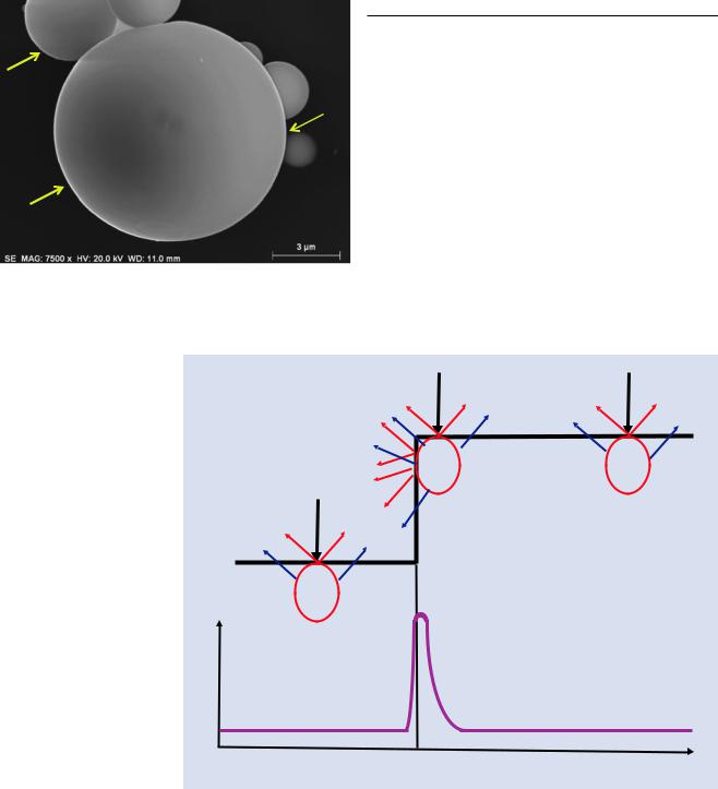
. Figs. 10.2 and 10.3 show an example of a group of
10.4.1\ SE Range Effects Produce Bright Edges (Isolated Edges)
. Fig. 10.3 SEM image of SRM 470 (Glass K -411) micro-particles prepared with an Everhart–Thornley detector(positive bias) and E0 = 20 keV. Note bright edges where the beam strikes tangentially
. Fig. 10.4 Schematic diagram showing behavior of BSE and SE signals as the beam approaches a vertical edge
SE1
SE2
Because of their extremely low kinetic energy of a few kilo- electronvolts, SEs have a short range of travel in a solid and thus can only escape from a shallow depth. The mean escape depth (SE range) is approximately 10 nm for a conductor.
When the beam is located in bulk material well away from edges, as shown schematically in . Fig. 10.4, the surface area from which SEs can escape is effectively constant as the beam is scanned, and the SE emission (SE1, SE2, and SE2) is thus constant and equal to the bulk SE coefficient appropriate to the target material at the local inclination angle. However, when the beam approaches an edge of a feature, such as the vertical wall shown in . Fig. 10.4, the escape of SEs is enhanced by the proximity of additional surface area that lies within the SE escape range. As the incident beam travels nearly parallel to the vertical face, the proximity of the surface along an extended portion of the beam path further enhances the escape of SEs, resulting in a very large
|
SE1 |
SE1 |
|
SE1 |
SE1 |
SE1 SE2 |
SE2 |
SE2 |
|
||
|
SE2 |
||||
|
|
|
|
|
|
SE2 |
|
|
|
|
|
SE1 |
|
|
|
|
|
SE1 |
SE1 |
|
|
|
|
SE2 |
|
|
|
|
|
SE2 |
|
|
|
|
|
SE signal
Scan position
\152 Chapter 10 · High Resolution Imaging
a |
|
b |
|
|
|
100 nm |
EHT = 5.00 kV |
Signal A = InLens |
Date :30 jul 2015 |
100 nm |
||
|
|
|
WD = 1.4 mm |
Mag = 151.08 K X |
Time :17:54:00 |
|
|
|
|
|
|||
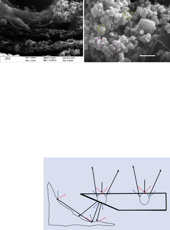
. Fig. 10.5 a SEM image at E0 = 5 keV of TiO2 particles using a through-the-lens detector for SE1 and SE2 (Bar = 100 nm). b Note bright edge effects and convergence of bright edges for the smallest particles (Example courtesy John Notte, Zeiss)
|
excess of SEs compared to the bulk interior. In addition, |
signal compared to bulk is a significant advantage. This is |
|
there will be enhanced escape of BSEs near the edge, and |
especially true considering the limitations that are imposed |
|
||
10 |
these BSEs will likely strike other nearby specimen and |
on high resolution performance by the demands of the |
|
instrument surfaces, producing even more SEs. All of the |
Threshold Current/Contrast Equation, as discussed below. |
|
signals collected when the beam is placed at a given scan |
|
|
location are assigned to that location in the image no matter |
10.4.2\ Even More Localized Signal: Edges |
|
where on the specimen or SEM chamber those signals are |
|
|
generated. The apparent SE emission coefficient when the |
Which Are Thin Relative to the Beam |
|
beam is placed near an edge is thus greatly increased over |
Range |
|
the bulk interior value, often by a factor of two to ten |
|
|
The enhanced SE escape near an edge shown in . Fig. 10.4 |
|
|
depending on the exact geometric circumstances. The edges |
|
|
of an object will appear very bright relative to the interior of |
is further increased when the beam approaches a feature |
|
the object, as shown in . Fig. 10.5 (e.g., objects in yellow |
edge that is thin enough for penetration of the beam elec- |
|
circles in . Fig. 10.5b) for particles of TiO2. Since the edges |
trons. As shown schematically in . Fig. 10.6, not only are |
|
are often the most important factor in defining a feature, a |
additional SEs generated as the beam electrons emerge as |
|
contrast mechanism that produces such an enhanced edge |
“BSEs” through the bottom and sides of the thin edge |
. Fig. 10.6 Schematic diagram of the enhanced BSE and SE production at an edge thin enough for beam penetration. BSEs may strike multiple surfaces, creating several generations of SEs
|
BSE |
|
|
BSE |
|
|
||
|
|
|
BSE |
|
BSE |
|||
|
|
|
|
|
|
|
||
|
|
|
|
|
|
|
|
|
|
|
|
SE1 |
|
SE1 |
SE1 SE |
|
|
SE2 |
SE |
2 |
SE1 |
SE2 |
2 |
|||
SE1 |
|
|
|
SE2 |
|
|
||
|
|
|
|
|
|
|
|
|
BSE |
|
|
|
|
|
|
|
|
BSE |
SE2 |
|
SE2 |
|
|
|
|
|
|
BSE |
|
|
|
|
|||
SE1 |
SE2 |
|
|
BSE |
SE1 |
|
|
|
|
|
|
|
|
|
|||
10.4 · Secondary Electron Contrast at High Spatial Resolution
structure, but these energetic BSEs will continue to travel, backscattering off other nearby specimen surfaces and the SEM lens and chamber walls, producing additional generations of SEs at each surface they strike. These additional SEs will be collected with significant efficiency by the E–T (positive bias) detector and assigned to each pixel as the beam approaches the edge, further increasing the signal at a thin edge relative to the interior and thus increasing the contrast of edges.
153 |
|
10 |
|
|
|
10.4.3\ Too Much of a Good Thing: The Bright
Edge Effect Can Hinder
Distinguishing Shape
As the dimensions of a free-standing object such as a particle or the diameter of a fiber approach the secondary electron escape length, the bright edge effects from two or more edges will converge, as shown schematically in . Fig. 10.7 and in the image of TiO2 particles (e.g., objects in magenta circles)
. Fig. 10.7 Convergence of bright edges as feature dimensions approach the SE escape distance. a Object edges separated by several multiples of the SE escape distance so that edge effects are distinct; b object edges sufficiently close for edge effects to begin to merge
a |
|
|
SE1 |
SE1 |
SE1 |
|
|
|
|
|
|||
|
|
|
SE1SE2 |
|
SE2 SE2 |
|
|
|
|
SE2 |
|
|
|
|
|
|
|
|
|
|
|
|
|
SE1 |
|
|
|
|
|
|
SE1 |
|
|
|
|
|
SE1 |
SE1 |
SE1 |
|
|
|
SE2 |
|
SE2 |
|
|
|
|
|
SE2 |
|
|
||
|
|
|
|
|
||
SE signal
Scan position
b |
|
|
SE1 SE1 |
|
|
|
|
||||
|
|
|
|
SE1 |
SE |
|
|
||||
|
|
|
SE1SE2 SE |
|
|
1 |
|
||||
|
|
|
2 |
|
SE2 |
|
|||||
|
|
|
|
|
|
|
|
|
SE2 |
||
|
|
|
SE2 |
|
|
|
|
|
|
|
SE1 |
|
|
|
|
|
|
|
|
|
|
||
|
|
|
|
|
|
|
|
|
|
SE2 |
|
|
|
|
SE1 |
|
|
|
|
|
|
|
|
|
|
|
|
|
|
|
|
|
|
|
|
|
|
|
SE1 |
|
|
|
|
|
|
SE1 |
|
|
|
|
|
|
|
|
|
|
|
|
|
|
|
SE1 |
SE1 |
SE1 |
|
|
|
|
|
SE1 |
|
|
SE2 |
|
SE |
2 |
|
|
|
|
SE |
2 |
|
|
|
SE2 |
|
|
|
|
|
||||
|
|
|
|
|
|
|
|
|
|
||
SE signal
 SE1
SE1
SE2
 SE1
SE1  SE2
SE2
 SE1
SE1
SE1 SE2
Scan position
\154 Chapter 10 · High Resolution Imaging
shown in . Fig. 10.5b. While the object will appear in high contrast as a very bright feature against the background, making it relatively easy to detect, as an object decreases in size it becomes difficult and eventually impossible to discern the true shape of an equiaxed object and to accurately measure its dimensions.
10.4.4\ Too Much of a Good Thing: The Bright Edge Effect Hinders Locating the True Position of an Edge for Critical Dimension Metrology
While the enhanced SE escape at an edge is a great advantage in visualizing the presence of an edge, the extreme signal excursion and its rapid change with beam position make it difficult to locate the absolute position of the edge within the
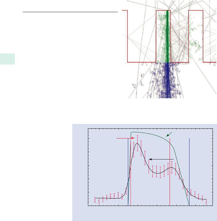
SE range, which can span 10 nm or even more for insulating materials. For advanced metrology applications such as semiconductor manufacturing critical dimension measurements where nanometer to sub-nanometer accuracy is required, detailed Monte Carlo modeling, as shown in . Fig. 10.8, of
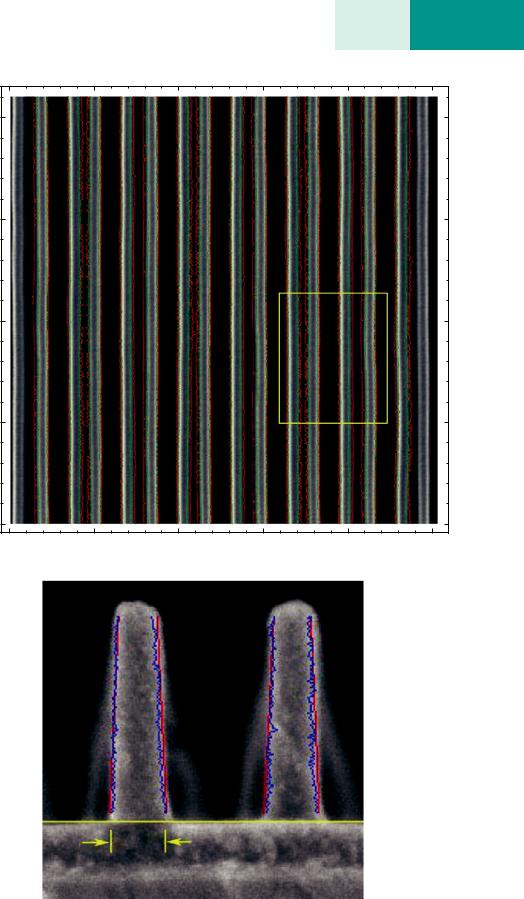
10 the beam electron, backscattered electron, and secondary electron trajectories as influenced by the specific geometry of the edge, is needed to deconvolve the measured signal profile as a function of scan position so as to recover the best estimate of the true edge location and object shape (NIST JMONSEL: Villarrubia et al. 2015). An example of an SEM signal profile across a structure and the shape recovered after deconvolution through modeling is shown in . Fig. 10.9. An application of this approach is shown in . Fig. 10.10, where a three-dimensional photoresist line was first imaged in a top-down SEM view (. Fig. 10.10a). Monte Carlo modeling applied to the signal profiles obtained from the top-down
view enabled a best fit estimate of the shape and dimensions of the line. The structure was subsequently cross-sectioned by ion beam milling to produce the SEM view shown in
. Fig. 10.10b. The best estimate of the structure obtained from the top-down imaging and modeling (red trace) is shown superimposed on the direct image of the cross-section edges (blue trace), showing excellent correspondence with this approach.
0.07 mm × 0.07 mm
. Fig. 10.8 Monte Carlo electron trajectory simulation of complex interactions at line-width structures as calculated with the J-MONSEL code (Villarrubia et al. 2015)
. Fig. 10.9 Application of J-MONSEL Monte Carlo simulation to measured SEM profile data and the estimated shape that best fits the data (Villarrubia et al. 2015)
Intensity(arb. units)
Best fit line shape
1.0 |
SEM intensity & |
|
uncertainty |
||
|
||
0.8 |
|
|
|
Best Intensity fit |
|
0.6 |
|
|
0.4 |
|
|
0.2 |
|
0.0
255 |
260 |
265 |
270 |
275 |
280 |
X (nm)
155 |
10 |
10.4 · Secondary Electron Contrast at High Spatial Resolution
. Fig. 10.10 a Top-down SEM |
a |
|
image of line-width test struc- |
||
|
||
tures; E0 = 15 keV. b Side view of |
400 |
structures revealed by focused |
|
|
ion beam milling showing esti- |
|
|
mated shape from modeling of |
|
|
the top-down image (red trace) |
|
|
compared with the edges directly |
|
|
found in the cross sectional |
|
|
image (blue) (Villarrubia et al. |
300 |
|
2015) |
||
|
# |
|
Linescan |
200 |
|
100
0
0 |
100 |
200 |
300 |
400 |
500 |
X (nm)
b
60 nm