

- •Preface
- •Imaging Microscopic Features
- •Measuring the Crystal Structure
- •References
- •Contents
- •1.4 Simulating the Effects of Elastic Scattering: Monte Carlo Calculations
- •What Are the Main Features of the Beam Electron Interaction Volume?
- •How Does the Interaction Volume Change with Composition?
- •How Does the Interaction Volume Change with Incident Beam Energy?
- •How Does the Interaction Volume Change with Specimen Tilt?
- •1.5 A Range Equation To Estimate the Size of the Interaction Volume
- •References
- •2: Backscattered Electrons
- •2.1 Origin
- •2.2.1 BSE Response to Specimen Composition (η vs. Atomic Number, Z)
- •SEM Image Contrast with BSE: “Atomic Number Contrast”
- •SEM Image Contrast: “BSE Topographic Contrast—Number Effects”
- •2.2.3 Angular Distribution of Backscattering
- •Beam Incident at an Acute Angle to the Specimen Surface (Specimen Tilt > 0°)
- •SEM Image Contrast: “BSE Topographic Contrast—Trajectory Effects”
- •2.2.4 Spatial Distribution of Backscattering
- •Depth Distribution of Backscattering
- •Radial Distribution of Backscattered Electrons
- •2.3 Summary
- •References
- •3: Secondary Electrons
- •3.1 Origin
- •3.2 Energy Distribution
- •3.3 Escape Depth of Secondary Electrons
- •3.8 Spatial Characteristics of Secondary Electrons
- •References
- •4: X-Rays
- •4.1 Overview
- •4.2 Characteristic X-Rays
- •4.2.1 Origin
- •4.2.2 Fluorescence Yield
- •4.2.3 X-Ray Families
- •4.2.4 X-Ray Nomenclature
- •4.2.6 Characteristic X-Ray Intensity
- •Isolated Atoms
- •X-Ray Production in Thin Foils
- •X-Ray Intensity Emitted from Thick, Solid Specimens
- •4.3 X-Ray Continuum (bremsstrahlung)
- •4.3.1 X-Ray Continuum Intensity
- •4.3.3 Range of X-ray Production
- •4.4 X-Ray Absorption
- •4.5 X-Ray Fluorescence
- •References
- •5.1 Electron Beam Parameters
- •5.2 Electron Optical Parameters
- •5.2.1 Beam Energy
- •Landing Energy
- •5.2.2 Beam Diameter
- •5.2.3 Beam Current
- •5.2.4 Beam Current Density
- •5.2.5 Beam Convergence Angle, α
- •5.2.6 Beam Solid Angle
- •5.2.7 Electron Optical Brightness, β
- •Brightness Equation
- •5.2.8 Focus
- •Astigmatism
- •5.3 SEM Imaging Modes
- •5.3.1 High Depth-of-Field Mode
- •5.3.2 High-Current Mode
- •5.3.3 Resolution Mode
- •5.3.4 Low-Voltage Mode
- •5.4 Electron Detectors
- •5.4.1 Important Properties of BSE and SE for Detector Design and Operation
- •Abundance
- •Angular Distribution
- •Kinetic Energy Response
- •5.4.2 Detector Characteristics
- •Angular Measures for Electron Detectors
- •Elevation (Take-Off) Angle, ψ, and Azimuthal Angle, ζ
- •Solid Angle, Ω
- •Energy Response
- •Bandwidth
- •5.4.3 Common Types of Electron Detectors
- •Backscattered Electrons
- •Passive Detectors
- •Scintillation Detectors
- •Semiconductor BSE Detectors
- •5.4.4 Secondary Electron Detectors
- •Everhart–Thornley Detector
- •Through-the-Lens (TTL) Electron Detectors
- •TTL SE Detector
- •TTL BSE Detector
- •Measuring the DQE: BSE Semiconductor Detector
- •References
- •6: Image Formation
- •6.1 Image Construction by Scanning Action
- •6.2 Magnification
- •6.3 Making Dimensional Measurements With the SEM: How Big Is That Feature?
- •Using a Calibrated Structure in ImageJ-Fiji
- •6.4 Image Defects
- •6.4.1 Projection Distortion (Foreshortening)
- •6.4.2 Image Defocusing (Blurring)
- •6.5 Making Measurements on Surfaces With Arbitrary Topography: Stereomicroscopy
- •6.5.1 Qualitative Stereomicroscopy
- •Fixed beam, Specimen Position Altered
- •Fixed Specimen, Beam Incidence Angle Changed
- •6.5.2 Quantitative Stereomicroscopy
- •Measuring a Simple Vertical Displacement
- •References
- •7: SEM Image Interpretation
- •7.1 Information in SEM Images
- •7.2.2 Calculating Atomic Number Contrast
- •Establishing a Robust Light-Optical Analogy
- •Getting It Wrong: Breaking the Light-Optical Analogy of the Everhart–Thornley (Positive Bias) Detector
- •Deconstructing the SEM/E–T Image of Topography
- •SUM Mode (A + B)
- •DIFFERENCE Mode (A−B)
- •References
- •References
- •9: Image Defects
- •9.1 Charging
- •9.1.1 What Is Specimen Charging?
- •9.1.3 Techniques to Control Charging Artifacts (High Vacuum Instruments)
- •Observing Uncoated Specimens
- •Coating an Insulating Specimen for Charge Dissipation
- •Choosing the Coating for Imaging Morphology
- •9.2 Radiation Damage
- •9.3 Contamination
- •References
- •10: High Resolution Imaging
- •10.2 Instrumentation Considerations
- •10.4.1 SE Range Effects Produce Bright Edges (Isolated Edges)
- •10.4.4 Too Much of a Good Thing: The Bright Edge Effect Hinders Locating the True Position of an Edge for Critical Dimension Metrology
- •10.5.1 Beam Energy Strategies
- •Low Beam Energy Strategy
- •High Beam Energy Strategy
- •Making More SE1: Apply a Thin High-δ Metal Coating
- •Making Fewer BSEs, SE2, and SE3 by Eliminating Bulk Scattering From the Substrate
- •10.6 Factors That Hinder Achieving High Resolution
- •10.6.2 Pathological Specimen Behavior
- •Contamination
- •Instabilities
- •References
- •11: Low Beam Energy SEM
- •11.3 Selecting the Beam Energy to Control the Spatial Sampling of Imaging Signals
- •11.3.1 Low Beam Energy for High Lateral Resolution SEM
- •11.3.2 Low Beam Energy for High Depth Resolution SEM
- •11.3.3 Extremely Low Beam Energy Imaging
- •References
- •12.1.1 Stable Electron Source Operation
- •12.1.2 Maintaining Beam Integrity
- •12.1.4 Minimizing Contamination
- •12.3.1 Control of Specimen Charging
- •12.5 VPSEM Image Resolution
- •References
- •13: ImageJ and Fiji
- •13.1 The ImageJ Universe
- •13.2 Fiji
- •13.3 Plugins
- •13.4 Where to Learn More
- •References
- •14: SEM Imaging Checklist
- •14.1.1 Conducting or Semiconducting Specimens
- •14.1.2 Insulating Specimens
- •14.2 Electron Signals Available
- •14.2.1 Beam Electron Range
- •14.2.2 Backscattered Electrons
- •14.2.3 Secondary Electrons
- •14.3 Selecting the Electron Detector
- •14.3.2 Backscattered Electron Detectors
- •14.3.3 “Through-the-Lens” Detectors
- •14.4 Selecting the Beam Energy for SEM Imaging
- •14.4.4 High Resolution SEM Imaging
- •Strategy 1
- •Strategy 2
- •14.5 Selecting the Beam Current
- •14.5.1 High Resolution Imaging
- •14.5.2 Low Contrast Features Require High Beam Current and/or Long Frame Time to Establish Visibility
- •14.6 Image Presentation
- •14.6.1 “Live” Display Adjustments
- •14.6.2 Post-Collection Processing
- •14.7 Image Interpretation
- •14.7.1 Observer’s Point of View
- •14.7.3 Contrast Encoding
- •14.8.1 VPSEM Advantages
- •14.8.2 VPSEM Disadvantages
- •15: SEM Case Studies
- •15.1 Case Study: How High Is That Feature Relative to Another?
- •15.2 Revealing Shallow Surface Relief
- •16.1.2 Minor Artifacts: The Si-Escape Peak
- •16.1.3 Minor Artifacts: Coincidence Peaks
- •16.1.4 Minor Artifacts: Si Absorption Edge and Si Internal Fluorescence Peak
- •16.2 “Best Practices” for Electron-Excited EDS Operation
- •16.2.1 Operation of the EDS System
- •Choosing the EDS Time Constant (Resolution and Throughput)
- •Choosing the Solid Angle of the EDS
- •Selecting a Beam Current for an Acceptable Level of System Dead-Time
- •16.3.1 Detector Geometry
- •16.3.2 Process Time
- •16.3.3 Optimal Working Distance
- •16.3.4 Detector Orientation
- •16.3.5 Count Rate Linearity
- •16.3.6 Energy Calibration Linearity
- •16.3.7 Other Items
- •16.3.8 Setting Up a Quality Control Program
- •Using the QC Tools Within DTSA-II
- •Creating a QC Project
- •Linearity of Output Count Rate with Live-Time Dose
- •Resolution and Peak Position Stability with Count Rate
- •Solid Angle for Low X-ray Flux
- •Maximizing Throughput at Moderate Resolution
- •References
- •17: DTSA-II EDS Software
- •17.1 Getting Started With NIST DTSA-II
- •17.1.1 Motivation
- •17.1.2 Platform
- •17.1.3 Overview
- •17.1.4 Design
- •Simulation
- •Quantification
- •Experiment Design
- •Modeled Detectors (. Fig. 17.1)
- •Window Type (. Fig. 17.2)
- •The Optimal Working Distance (. Figs. 17.3 and 17.4)
- •Elevation Angle
- •Sample-to-Detector Distance
- •Detector Area
- •Crystal Thickness
- •Number of Channels, Energy Scale, and Zero Offset
- •Resolution at Mn Kα (Approximate)
- •Azimuthal Angle
- •Gold Layer, Aluminum Layer, Nickel Layer
- •Dead Layer
- •Zero Strobe Discriminator (. Figs. 17.7 and 17.8)
- •Material Editor Dialog (. Figs. 17.9, 17.10, 17.11, 17.12, 17.13, and 17.14)
- •17.2.1 Introduction
- •17.2.2 Monte Carlo Simulation
- •17.2.4 Optional Tables
- •References
- •18: Qualitative Elemental Analysis by Energy Dispersive X-Ray Spectrometry
- •18.1 Quality Assurance Issues for Qualitative Analysis: EDS Calibration
- •18.2 Principles of Qualitative EDS Analysis
- •Exciting Characteristic X-Rays
- •Fluorescence Yield
- •X-ray Absorption
- •Si Escape Peak
- •Coincidence Peaks
- •18.3 Performing Manual Qualitative Analysis
- •Beam Energy
- •Choosing the EDS Resolution (Detector Time Constant)
- •Obtaining Adequate Counts
- •18.4.1 Employ the Available Software Tools
- •18.4.3 Lower Photon Energy Region
- •18.4.5 Checking Your Work
- •18.5 A Worked Example of Manual Peak Identification
- •References
- •19.1 What Is a k-ratio?
- •19.3 Sets of k-ratios
- •19.5 The Analytical Total
- •19.6 Normalization
- •19.7.1 Oxygen by Assumed Stoichiometry
- •19.7.3 Element by Difference
- •19.8 Ways of Reporting Composition
- •19.8.1 Mass Fraction
- •19.8.2 Atomic Fraction
- •19.8.3 Stoichiometry
- •19.8.4 Oxide Fractions
- •Example Calculations
- •19.9 The Accuracy of Quantitative Electron-Excited X-ray Microanalysis
- •19.9.1 Standards-Based k-ratio Protocol
- •19.9.2 “Standardless Analysis”
- •19.10 Appendix
- •19.10.1 The Need for Matrix Corrections To Achieve Quantitative Analysis
- •19.10.2 The Physical Origin of Matrix Effects
- •19.10.3 ZAF Factors in Microanalysis
- •X-ray Generation With Depth, φ(ρz)
- •X-ray Absorption Effect, A
- •X-ray Fluorescence, F
- •References
- •20.2 Instrumentation Requirements
- •20.2.1 Choosing the EDS Parameters
- •EDS Spectrum Channel Energy Width and Spectrum Energy Span
- •EDS Time Constant (Resolution and Throughput)
- •EDS Calibration
- •EDS Solid Angle
- •20.2.2 Choosing the Beam Energy, E0
- •20.2.3 Measuring the Beam Current
- •20.2.4 Choosing the Beam Current
- •Optimizing Analysis Strategy
- •20.3.4 Ba-Ti Interference in BaTiSi3O9
- •20.4 The Need for an Iterative Qualitative and Quantitative Analysis Strategy
- •20.4.2 Analysis of a Stainless Steel
- •20.5 Is the Specimen Homogeneous?
- •20.6 Beam-Sensitive Specimens
- •20.6.1 Alkali Element Migration
- •20.6.2 Materials Subject to Mass Loss During Electron Bombardment—the Marshall-Hall Method
- •Thin Section Analysis
- •Bulk Biological and Organic Specimens
- •References
- •21: Trace Analysis by SEM/EDS
- •21.1 Limits of Detection for SEM/EDS Microanalysis
- •21.2.1 Estimating CDL from a Trace or Minor Constituent from Measuring a Known Standard
- •21.2.2 Estimating CDL After Determination of a Minor or Trace Constituent with Severe Peak Interference from a Major Constituent
- •21.3 Measurements of Trace Constituents by Electron-Excited Energy Dispersive X-ray Spectrometry
- •The Inevitable Physics of Remote Excitation Within the Specimen: Secondary Fluorescence Beyond the Electron Interaction Volume
- •Simulation of Long-Range Secondary X-ray Fluorescence
- •NIST DTSA II Simulation: Vertical Interface Between Two Regions of Different Composition in a Flat Bulk Target
- •NIST DTSA II Simulation: Cubic Particle Embedded in a Bulk Matrix
- •21.5 Summary
- •References
- •22.1.2 Low Beam Energy Analysis Range
- •22.2 Advantage of Low Beam Energy X-Ray Microanalysis
- •22.2.1 Improved Spatial Resolution
- •22.3 Challenges and Limitations of Low Beam Energy X-Ray Microanalysis
- •22.3.1 Reduced Access to Elements
- •22.3.3 At Low Beam Energy, Almost Everything Is Found To Be Layered
- •Analysis of Surface Contamination
- •References
- •23: Analysis of Specimens with Special Geometry: Irregular Bulk Objects and Particles
- •23.2.1 No Chemical Etching
- •23.3 Consequences of Attempting Analysis of Bulk Materials With Rough Surfaces
- •23.4.1 The Raw Analytical Total
- •23.4.2 The Shape of the EDS Spectrum
- •23.5 Best Practices for Analysis of Rough Bulk Samples
- •23.6 Particle Analysis
- •Particle Sample Preparation: Bulk Substrate
- •The Importance of Beam Placement
- •Overscanning
- •“Particle Mass Effect”
- •“Particle Absorption Effect”
- •The Analytical Total Reveals the Impact of Particle Effects
- •Does Overscanning Help?
- •23.6.6 Peak-to-Background (P/B) Method
- •Specimen Geometry Severely Affects the k-ratio, but Not the P/B
- •Using the P/B Correspondence
- •23.7 Summary
- •References
- •24: Compositional Mapping
- •24.2 X-Ray Spectrum Imaging
- •24.2.1 Utilizing XSI Datacubes
- •24.2.2 Derived Spectra
- •SUM Spectrum
- •MAXIMUM PIXEL Spectrum
- •24.3 Quantitative Compositional Mapping
- •24.4 Strategy for XSI Elemental Mapping Data Collection
- •24.4.1 Choosing the EDS Dead-Time
- •24.4.2 Choosing the Pixel Density
- •24.4.3 Choosing the Pixel Dwell Time
- •“Flash Mapping”
- •High Count Mapping
- •References
- •25.1 Gas Scattering Effects in the VPSEM
- •25.1.1 Why Doesn’t the EDS Collimator Exclude the Remote Skirt X-Rays?
- •25.2 What Can Be Done To Minimize gas Scattering in VPSEM?
- •25.2.2 Favorable Sample Characteristics
- •Particle Analysis
- •25.2.3 Unfavorable Sample Characteristics
- •References
- •26.1 Instrumentation
- •26.1.2 EDS Detector
- •26.1.3 Probe Current Measurement Device
- •Direct Measurement: Using a Faraday Cup and Picoammeter
- •A Faraday Cup
- •Electrically Isolated Stage
- •Indirect Measurement: Using a Calibration Spectrum
- •26.1.4 Conductive Coating
- •26.2 Sample Preparation
- •26.2.1 Standard Materials
- •26.2.2 Peak Reference Materials
- •26.3 Initial Set-Up
- •26.3.1 Calibrating the EDS Detector
- •Selecting a Pulse Process Time Constant
- •Energy Calibration
- •Quality Control
- •Sample Orientation
- •Detector Position
- •Probe Current
- •26.4 Collecting Data
- •26.4.1 Exploratory Spectrum
- •26.4.2 Experiment Optimization
- •26.4.3 Selecting Standards
- •26.4.4 Reference Spectra
- •26.4.5 Collecting Standards
- •26.4.6 Collecting Peak-Fitting References
- •26.5 Data Analysis
- •26.5.2 Quantification
- •26.6 Quality Check
- •Reference
- •27.2 Case Study: Aluminum Wire Failures in Residential Wiring
- •References
- •28: Cathodoluminescence
- •28.1 Origin
- •28.2 Measuring Cathodoluminescence
- •28.3 Applications of CL
- •28.3.1 Geology
- •Carbonado Diamond
- •Ancient Impact Zircons
- •28.3.2 Materials Science
- •Semiconductors
- •Lead-Acid Battery Plate Reactions
- •28.3.3 Organic Compounds
- •References
- •29.1.1 Single Crystals
- •29.1.2 Polycrystalline Materials
- •29.1.3 Conditions for Detecting Electron Channeling Contrast
- •Specimen Preparation
- •Instrument Conditions
- •29.2.1 Origin of EBSD Patterns
- •29.2.2 Cameras for EBSD Pattern Detection
- •29.2.3 EBSD Spatial Resolution
- •29.2.5 Steps in Typical EBSD Measurements
- •Sample Preparation for EBSD
- •Align Sample in the SEM
- •Check for EBSD Patterns
- •Adjust SEM and Select EBSD Map Parameters
- •Run the Automated Map
- •29.2.6 Display of the Acquired Data
- •29.2.7 Other Map Components
- •29.2.10 Application Example
- •Application of EBSD To Understand Meteorite Formation
- •29.2.11 Summary
- •Specimen Considerations
- •EBSD Detector
- •Selection of Candidate Crystallographic Phases
- •Microscope Operating Conditions and Pattern Optimization
- •Selection of EBSD Acquisition Parameters
- •Collect the Orientation Map
- •References
- •30.1 Introduction
- •30.2 Ion–Solid Interactions
- •30.3 Focused Ion Beam Systems
- •30.5 Preparation of Samples for SEM
- •30.5.1 Cross-Section Preparation
- •30.5.2 FIB Sample Preparation for 3D Techniques and Imaging
- •30.6 Summary
- •References
- •31: Ion Beam Microscopy
- •31.1 What Is So Useful About Ions?
- •31.2 Generating Ion Beams
- •31.3 Signal Generation in the HIM
- •31.5 Patterning with Ion Beams
- •31.7 Chemical Microanalysis with Ion Beams
- •References
- •Appendix
- •A Database of Electron–Solid Interactions
- •A Database of Electron–Solid Interactions
- •Introduction
- •Backscattered Electrons
- •Secondary Yields
- •Stopping Powers
- •X-ray Ionization Cross Sections
- •Conclusions
- •References
- •Index
- •Reference List
- •Index

341 |
|
21 |
|
|
|
Trace Analysis by SEM/EDS
21.1\ Limits of Detection for SEM/EDS Microanalysis – 342
21.2\ Estimating the Concentration Limit of Detection, CDL – 343
21.2.1Estimating CDL from a Trace or Minor Constituent from Measuring a Known Standard – 343
21.2.2Estimating CDL After Determination of a Minor or Trace Constituent with Severe Peak Interference from a Major Constituent – 343
21.2.3Estimating CDL When a Reference Value for Trace or Minor Element Is Not Available – 343
21.3\ Measurements of Trace Constituents by Electron-Excited Energy Dispersive X-ray Spectrometry – 345
21.3.1\ Is a Given Trace Level Measurement Actually Valid? – 345
21.4\ Pathological Electron Scattering Can Produce “Trace” Contributions to EDS Spectra – 350
21.4.1\ Instrumental Sources of Trace Analysis Artifacts – 350
21.4.2\ Assessing Remote Excitation Sources in an SEM-EDS System – 353
21.5\ Summary – 357
\References – 357
© Springer Science+Business Media LLC 2018
J. Goldstein et al., Scanning Electron Microscopy and X-Ray Microanalysis, https://doi.org/10.1007/978-1-4939-6676-9_21
\342 Chapter 21 · Trace Analysis by SEM/EDS
“Trace analysis” refers to the measurement of constituents presents at low fractional levels. For SEM/EDS the following arbitrary but practical definitions have been chosen to designate various constituent classes according to these mass concentration (C) ranges:
Major: C> 0.1 mass fraction (greater than 10 wt%) Minor: 0.01 ≤C≤0.1 (1 wt% to 10 wt%)
Trace: C< 0.01 (below 1 wt%)
Note that by these definitions, while “major” and “minor” constituents have defined ranges, “trace” has no minimum. Strictly, the presence of a single atom of the element of interest within the electron-excited mass that is analyzed by X-ray spectrometry represents the ultimate trace level that might be measured for that species, but such detection is far below the practical limit for electron-excited energy dispersive X-ray spectrometry of bulk specimens. In this section trace analysis down to levels approaching a mass fraction of C= 0.0001 (100 ppm (ppm) will be demonstrated. While such trace measurements are possible with high count EDS spectra, achieving reliable trace measurements by electron-excited energy dispersive X-ray spectrometry requires careful attention to identifying and eliminating, if possible, pathological contributions to the measured spectrum from unexpected remote radiation sources such as secondary fluorescence and backscattered electrons (Newbury and Ritchie 2016).
21.1\ Limits of Detection for SEM/EDS Microanalysis
How does the measured EDS X-ray intensity (counts in the energy window) for an element behave for constituents in the trace regime? As described in the modules on X-ray physics and on quantitative X-ray microanalysis, the X-ray spectrum that is measured is a result of the complex physics of electron- excited X-ray generation and of subsequent propagation of X-rays through the specimen to reach the EDS spectrometer. The intensity measured for the characteristic X-rays of a particular element in the excited volume is affected by all other elements present, creating the so-called matrix effects: (1) the atomic number effect that depends on the rate of electron energy loss and on the number of backscattered electrons and the BSE energy distribution; (2) the absorption effect, where the mass absorption coefficient depends on all elements present; and (3) the secondary fluorescence effect, where the absorption of characteristic and continuum X-rays with photon energies above the ionization energy of the element of
21 interest leads to additional emission for that element. Consider the number of X-rays, NA, including characteristic plus continuum, measured in the energy window that spans the peak for element “A” as a function of the concentration CA in a specific mixture of other elements “B,” “C,” “D,” and so on. A simple example would be a binary alloy system where there is complete solid solubility from pure “A” to pure “B,” for
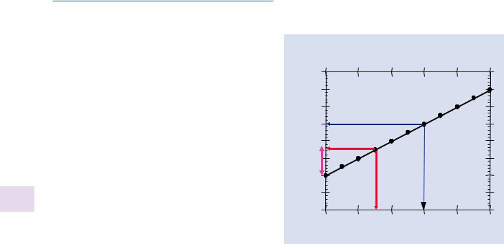
example, Au-Cu or Au-Ag. When element “A” is present as a major constituent, as the concentration of “A” is reduced and replaced by “B,” the matrix effects are likely to change significantly as the composition is changed. The impact of “B” on electron scattering and X-ray absorption of “A” is likely to produce a complex and non-linear response for NA as a function of CA. However, when the element of interest “A” is present in the trace concentration range, the matrix composition is very nearly constant as the concentration of “A” is lowered and replaced by “B,” resulting in a monotonic dependence for NA as a function of CA, as shown in . Fig. 21.1, known as a “working curve,” which in the case of a dilute constituent will be linear. Consider that we have a known point on this linear plot with the values (Ns, Cs) in the trace concentration range that corresponds to the measurement of a known standard or is the result of a quantitative analysis of an unknown. The slope m of this linear function can be calculated from this known point and the 0 concentration point, for which NA =0+Ncm, since there will still be counts, Ncm, in the “A” energy window due to the X-ray continuum produced by the other element(s) that comprise the specimen:
slope = (Ns − Ncm ) / (Cs − 0) |
\ |
(21.1) |
|
|
The slope-intercept form (y= mx + b) for the linear expression for the X-ray counts in the “A” energy window, NA, as a function of concentration, CA, can then be constructed as:
N |
A |
= |
N |
s |
− N |
cm ) |
/ |
( |
C − 0 |
C |
A |
+ N |
cm |
(21.2) |
|
( |
|
|
|
s |
) |
|
|
||||||
|
|
|
|
|
|
|
|
|
|
|
|
|
\ |
|
The y-axis intercept, b, is equal to Ncm, as shown in . Fig. 21.1. Because of the presence of the continuum background at all
y = mx +b
NA = [(Ns – Ncm)/(Cs – 0)]Ca + Ncm
(Ns, Cs)
A |
Ns |
|
|
N |
|
(NDL,CDL) |
|
Counts, |
? |
|
|
|
NDL |
|
|
|
Ncm |
|
|
|
0 |
CDL |
Cs |
Concentration, CA
. Fig. 21.1 Linear working curve for a constituent at low concentration in an effectively constant matrix

21.2 · Estimating the Concentration Limit of Detection, CDL
photon energies, the concentration limit of detection, CDL, must have a finite, non-zero value that will be found at some point (NDL, CDL) along the linear response between (Ncm, 0) and (Ns, Cs). The work of (Currie 1968) can be used to define the condition at which the counts from the characteristic X-ray emission can be distinguished with a high degree of confidence above the natural statistical fluctuations in the background counts: the characteristic counts must exceed three times the standard deviation of the background:
N |
A |
> 3 N½ |
(21.3) |
|
cm \ |
|
Thus, at the concentration limit of detection, CDL:
NDL = continuum + characteristic = Ncm + 3 Ncm½ \ (21.4a)
N |
DL |
−N |
cm |
= 3 N½ |
(21.4b) |
|
|
cm \ |
|
Substituting these conditions for (NDL, CDL) in Eq. (21.2):
|
|
N |
DL |
= |
N |
s |
− N |
cm ) |
/ |
( |
C − |
0 |
C |
DL |
+ N |
cm |
|
(21.5a) |
|||||||||||
|
|
|
|
|
( |
|
|
|
|
|
|
|
s |
|
) |
|
|
|
|
|
|||||||||
|
|
|
|
|
|
|
|
|
|
|
|
|
|
|
|
|
|
|
|
|
|
|
|
|
|
|
\ |
|
|
N |
DL |
− N |
cm |
= 3 N½ |
|
= |
N |
s |
− N |
cm ) |
/ |
( |
C − 0 |
C |
DL |
(21.5b) |
|||||||||||||
|
|
|
|
|
|
|
cm |
|
( |
|
|
|
|
|
s |
|
|
) |
|
||||||||||
|
|
|
|
|
|
|
|
|
|
|
|
|
|
|
|
|
|
|
|
|
|
|
|
|
|
|
|
\ |
|
|
|
C |
DL |
= 3 N½ |
/ |
( |
N |
s |
− N |
C |
|
|
|
|
|
|
|
(21.5c) |
|||||||||||
|
|
|
|
|
|
cm |
|
|
|
|
|
|
|
cm ) |
s |
\ |
|
|
|
|
|
|
|
||||||
|
|
|
|
|
|
|
|
|
|
|
|
|
|
|
|
|
|
|
|
|
|
|
|
|
|
|
|
|
|
Equation (21.5c) enables estimation of CDL from the results of a single analysis of an unknown or from a single measurement of a known standard to provide a value for Cs. The corresponding measured EDS spectrum is used to determine Ns and Ncm. If n repeated measurements are made, Ns and Ncm are then taken as averages, Ṅs and Ṅcm, over the n measurements, and Eq. (21.5c) becomes
½ |
|
|
1/2 |
|
(21.6) |
CDL = 3 Ncm |
/ (Ns |
− Ncm )n |
Cs |
||
|
|
|
|
|
\ |
CDL is an estimate of the concentration level of a constituent that can just be detected with a high degree of confidence. Quantification at CDL is not reasonable because the error budget is dominated by the variance of the continuum. To achieve meaningful quantitation of trace constituents, (Currie 1968) further defines a minimum quantifiable concentration, CMQ, which requires that the characteristic intensity exceed 10 Ncm½: Inserting this criterion in Eq. 21.5c gives
C |
MQ |
= 10 N½ |
/ |
( |
N |
s |
− N |
C |
|
(21.7) |
||
|
|
cm |
|
|
|
cm ) |
s |
|
||||
|
|
|
|
|
|
|
|
|
|
|
\ |
|
343 |
|
21 |
|
|
|
21.2.1\ Estimating CDL from a Trace or Minor Constituent from Measuring a Known Standard
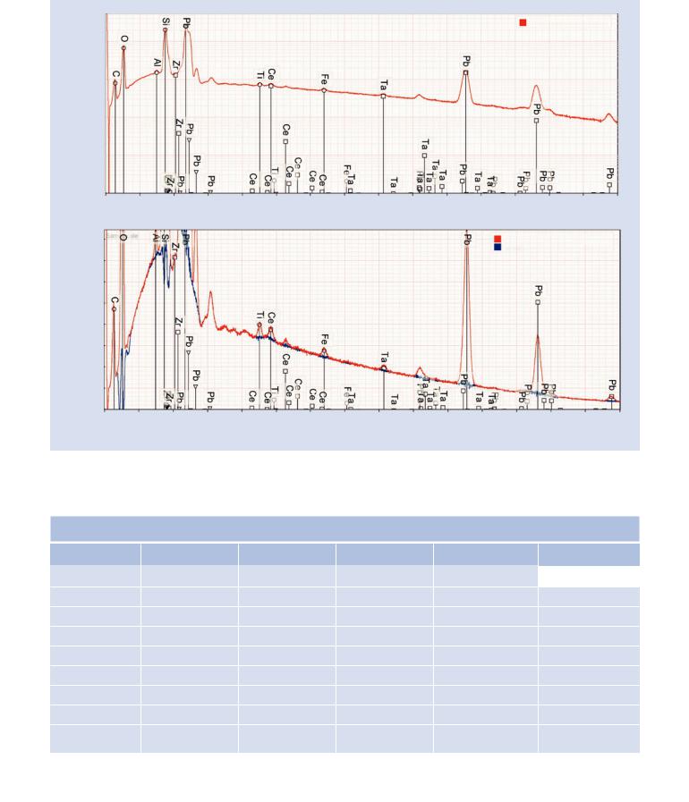
. Figure 21.2 shows a high count silicon drift detector (SDD)-EDS spectrum of K493 (and the residual spectrum after fitting for O, Si, and Pb), in NIST Research Material glass with the composition (as-synthesized) listed in
. Table 21.1. . Table 21.1 also lists the measured peak intensity Ns and the background Ncm determined for this spectrum with the EDS spectrum measurement tools in DTSA-II. For a single measurement, the values for Cs, Ns, and Ncm inserted in Eq. (21.5c) gives the estimate of CDL for each trace element, as also listed in . Table 21.1. If n= 4 repeated measurements were made (or a single measurement was performed at four times the dose), CDL would be lowered by a factor of 2. Examination of the values for CDL in . Table 21.1 reveals more than an order-of-magnitude variation depending on atomic number, for example, CDL = 52 ppm for Al while CDL = 754 ppm for Ta. This strong variation arises from differences in the relative excitation (overvoltage) and fluorescence yield for the various elements, differences in the continuum intensity, and the partitioning of the characteristic X-ray intensity among widely separated peaks for the L-family of the higher atomic number elements, for example, Ce and Ta.
21.2.2\ Estimating CDL After Determination of a Minor or Trace Constituent with Severe Peak Interference from a Major Constituent
Because of the relatively poor energy resolution of EDS, peak interference situations are frequently encountered. Multiple linear least squares peak fitting can separate the contributions from two or more peaks within an energy window. This effect is illustrated in . Fig. 21.3 for Corning Glass A, the composition of which is listed in . Table 21.2 along with the DTSA II analysis. There is a significant interference for K and Ca upon Sb and Sn. The initial qualitative analysis identified K and Ca, as shown in . Fig. 21.3(a). When MLLS peak fitting is applied for K and Ca, the Sn and Sb L-family peaks are revealed in the residual spectrum, . Fig. 21.3(b). The limit of detection calculated from the peak for Sn L determined from peak and background intensities determined from this residual spectrum is CDL = 0.00002 (200 ppm).
21.2\ Estimating the Concentration Limit |
21.2.3\ Estimating CDL When a Reference |
of Detection, CDL |
Value for Trace or Minor Element Is |
|
Not Available |
|
Equation (21.5c) or (21.6), as appropriate to single or multiple repeated measurements, can be used to estimate the concentration limit of detection for various situations.
Another type of problem that may be encountered is the situation where the analyst wishes to estimate CDL for hypothetical
\344 Chapter 21 · Trace Analysis by SEM/EDS
Counts
Counts
10 0000
10 000
1000
100
10
0.0
16 000
14 000
12 000
10 000
8 000
6 000
4 000
2 000
0
0.0
K493_20kV10nA11%DT200s
K493
E0 = 20 keV
0.1-20 keV = 15.1 million counts
1.0 |
2.0 |
3.0 |
4.0 |
5.0 |
6.0 |
7.0 |
8.0 |
9.0 |
10.0 |
11.0 |
12.0 |
13.0 |
14.0 |
15.0 |
Photon energy (keV)
K493_20kV10nA11%DT200s
Residual[K493_20kV10nA11%DT200s]
K493
Residual after peak fitting
1.0 |
2.0 |
3.0 |
4.0 |
5.0 |
6.0 |
7.0 |
8.0 |
9.0 |
10.0 |
11.0 |
12.0 |
13.0 |
14.0 |
15.0 |
Photon energy (keV)
. Fig. 21.2 SDD-EDS spectrum (0.1–20 keV = 29 million counts) of NIST Research Material Glass K493 at E0 = 20 keV and residual after MLLS peak fitting for O, Si, and Pb
. Table 21.1 Limits of detection estimated from a known standard K493 (E0 = 20 keV 0.1–20 keV = 29 million counts)
|
Element |
Mass conc |
Ns (counts) |
Ncm (counts) |
CDL (mass conc) |
CDL (ppm) |
|
|
O |
0.2063 |
|
|
|
|
|
|
|
|
|
|
|
|
|
|
Al |
0.00106 |
434,999 |
396,617 |
0.000052 |
52 ppm |
|
|
Si |
0.1304 |
|
|
|
|
|
|
Ti |
0.00192 |
280,709 |
255,991 |
0.000118 |
118 ppm |
|
|
Fe |
0.00224 |
229,356 |
210,799 |
0.000166 |
166 ppm |
|
|
Zr |
0.00363 |
313,728 |
303,760 |
0.000602 |
602 ppm |
|
21 |
|||||||
Ce (L) |
0.00554 |
291,575 |
269,042 |
0.000383 |
383 ppm |
||
|
Ta (L) |
0.00721 |
156,283 |
145,340 |
0.000754 |
754 ppm |
|
|
|||||||
|
Pb |
0.6413 |
|
|
|
|