

- •Preface
- •Imaging Microscopic Features
- •Measuring the Crystal Structure
- •References
- •Contents
- •1.4 Simulating the Effects of Elastic Scattering: Monte Carlo Calculations
- •What Are the Main Features of the Beam Electron Interaction Volume?
- •How Does the Interaction Volume Change with Composition?
- •How Does the Interaction Volume Change with Incident Beam Energy?
- •How Does the Interaction Volume Change with Specimen Tilt?
- •1.5 A Range Equation To Estimate the Size of the Interaction Volume
- •References
- •2: Backscattered Electrons
- •2.1 Origin
- •2.2.1 BSE Response to Specimen Composition (η vs. Atomic Number, Z)
- •SEM Image Contrast with BSE: “Atomic Number Contrast”
- •SEM Image Contrast: “BSE Topographic Contrast—Number Effects”
- •2.2.3 Angular Distribution of Backscattering
- •Beam Incident at an Acute Angle to the Specimen Surface (Specimen Tilt > 0°)
- •SEM Image Contrast: “BSE Topographic Contrast—Trajectory Effects”
- •2.2.4 Spatial Distribution of Backscattering
- •Depth Distribution of Backscattering
- •Radial Distribution of Backscattered Electrons
- •2.3 Summary
- •References
- •3: Secondary Electrons
- •3.1 Origin
- •3.2 Energy Distribution
- •3.3 Escape Depth of Secondary Electrons
- •3.8 Spatial Characteristics of Secondary Electrons
- •References
- •4: X-Rays
- •4.1 Overview
- •4.2 Characteristic X-Rays
- •4.2.1 Origin
- •4.2.2 Fluorescence Yield
- •4.2.3 X-Ray Families
- •4.2.4 X-Ray Nomenclature
- •4.2.6 Characteristic X-Ray Intensity
- •Isolated Atoms
- •X-Ray Production in Thin Foils
- •X-Ray Intensity Emitted from Thick, Solid Specimens
- •4.3 X-Ray Continuum (bremsstrahlung)
- •4.3.1 X-Ray Continuum Intensity
- •4.3.3 Range of X-ray Production
- •4.4 X-Ray Absorption
- •4.5 X-Ray Fluorescence
- •References
- •5.1 Electron Beam Parameters
- •5.2 Electron Optical Parameters
- •5.2.1 Beam Energy
- •Landing Energy
- •5.2.2 Beam Diameter
- •5.2.3 Beam Current
- •5.2.4 Beam Current Density
- •5.2.5 Beam Convergence Angle, α
- •5.2.6 Beam Solid Angle
- •5.2.7 Electron Optical Brightness, β
- •Brightness Equation
- •5.2.8 Focus
- •Astigmatism
- •5.3 SEM Imaging Modes
- •5.3.1 High Depth-of-Field Mode
- •5.3.2 High-Current Mode
- •5.3.3 Resolution Mode
- •5.3.4 Low-Voltage Mode
- •5.4 Electron Detectors
- •5.4.1 Important Properties of BSE and SE for Detector Design and Operation
- •Abundance
- •Angular Distribution
- •Kinetic Energy Response
- •5.4.2 Detector Characteristics
- •Angular Measures for Electron Detectors
- •Elevation (Take-Off) Angle, ψ, and Azimuthal Angle, ζ
- •Solid Angle, Ω
- •Energy Response
- •Bandwidth
- •5.4.3 Common Types of Electron Detectors
- •Backscattered Electrons
- •Passive Detectors
- •Scintillation Detectors
- •Semiconductor BSE Detectors
- •5.4.4 Secondary Electron Detectors
- •Everhart–Thornley Detector
- •Through-the-Lens (TTL) Electron Detectors
- •TTL SE Detector
- •TTL BSE Detector
- •Measuring the DQE: BSE Semiconductor Detector
- •References
- •6: Image Formation
- •6.1 Image Construction by Scanning Action
- •6.2 Magnification
- •6.3 Making Dimensional Measurements With the SEM: How Big Is That Feature?
- •Using a Calibrated Structure in ImageJ-Fiji
- •6.4 Image Defects
- •6.4.1 Projection Distortion (Foreshortening)
- •6.4.2 Image Defocusing (Blurring)
- •6.5 Making Measurements on Surfaces With Arbitrary Topography: Stereomicroscopy
- •6.5.1 Qualitative Stereomicroscopy
- •Fixed beam, Specimen Position Altered
- •Fixed Specimen, Beam Incidence Angle Changed
- •6.5.2 Quantitative Stereomicroscopy
- •Measuring a Simple Vertical Displacement
- •References
- •7: SEM Image Interpretation
- •7.1 Information in SEM Images
- •7.2.2 Calculating Atomic Number Contrast
- •Establishing a Robust Light-Optical Analogy
- •Getting It Wrong: Breaking the Light-Optical Analogy of the Everhart–Thornley (Positive Bias) Detector
- •Deconstructing the SEM/E–T Image of Topography
- •SUM Mode (A + B)
- •DIFFERENCE Mode (A−B)
- •References
- •References
- •9: Image Defects
- •9.1 Charging
- •9.1.1 What Is Specimen Charging?
- •9.1.3 Techniques to Control Charging Artifacts (High Vacuum Instruments)
- •Observing Uncoated Specimens
- •Coating an Insulating Specimen for Charge Dissipation
- •Choosing the Coating for Imaging Morphology
- •9.2 Radiation Damage
- •9.3 Contamination
- •References
- •10: High Resolution Imaging
- •10.2 Instrumentation Considerations
- •10.4.1 SE Range Effects Produce Bright Edges (Isolated Edges)
- •10.4.4 Too Much of a Good Thing: The Bright Edge Effect Hinders Locating the True Position of an Edge for Critical Dimension Metrology
- •10.5.1 Beam Energy Strategies
- •Low Beam Energy Strategy
- •High Beam Energy Strategy
- •Making More SE1: Apply a Thin High-δ Metal Coating
- •Making Fewer BSEs, SE2, and SE3 by Eliminating Bulk Scattering From the Substrate
- •10.6 Factors That Hinder Achieving High Resolution
- •10.6.2 Pathological Specimen Behavior
- •Contamination
- •Instabilities
- •References
- •11: Low Beam Energy SEM
- •11.3 Selecting the Beam Energy to Control the Spatial Sampling of Imaging Signals
- •11.3.1 Low Beam Energy for High Lateral Resolution SEM
- •11.3.2 Low Beam Energy for High Depth Resolution SEM
- •11.3.3 Extremely Low Beam Energy Imaging
- •References
- •12.1.1 Stable Electron Source Operation
- •12.1.2 Maintaining Beam Integrity
- •12.1.4 Minimizing Contamination
- •12.3.1 Control of Specimen Charging
- •12.5 VPSEM Image Resolution
- •References
- •13: ImageJ and Fiji
- •13.1 The ImageJ Universe
- •13.2 Fiji
- •13.3 Plugins
- •13.4 Where to Learn More
- •References
- •14: SEM Imaging Checklist
- •14.1.1 Conducting or Semiconducting Specimens
- •14.1.2 Insulating Specimens
- •14.2 Electron Signals Available
- •14.2.1 Beam Electron Range
- •14.2.2 Backscattered Electrons
- •14.2.3 Secondary Electrons
- •14.3 Selecting the Electron Detector
- •14.3.2 Backscattered Electron Detectors
- •14.3.3 “Through-the-Lens” Detectors
- •14.4 Selecting the Beam Energy for SEM Imaging
- •14.4.4 High Resolution SEM Imaging
- •Strategy 1
- •Strategy 2
- •14.5 Selecting the Beam Current
- •14.5.1 High Resolution Imaging
- •14.5.2 Low Contrast Features Require High Beam Current and/or Long Frame Time to Establish Visibility
- •14.6 Image Presentation
- •14.6.1 “Live” Display Adjustments
- •14.6.2 Post-Collection Processing
- •14.7 Image Interpretation
- •14.7.1 Observer’s Point of View
- •14.7.3 Contrast Encoding
- •14.8.1 VPSEM Advantages
- •14.8.2 VPSEM Disadvantages
- •15: SEM Case Studies
- •15.1 Case Study: How High Is That Feature Relative to Another?
- •15.2 Revealing Shallow Surface Relief
- •16.1.2 Minor Artifacts: The Si-Escape Peak
- •16.1.3 Minor Artifacts: Coincidence Peaks
- •16.1.4 Minor Artifacts: Si Absorption Edge and Si Internal Fluorescence Peak
- •16.2 “Best Practices” for Electron-Excited EDS Operation
- •16.2.1 Operation of the EDS System
- •Choosing the EDS Time Constant (Resolution and Throughput)
- •Choosing the Solid Angle of the EDS
- •Selecting a Beam Current for an Acceptable Level of System Dead-Time
- •16.3.1 Detector Geometry
- •16.3.2 Process Time
- •16.3.3 Optimal Working Distance
- •16.3.4 Detector Orientation
- •16.3.5 Count Rate Linearity
- •16.3.6 Energy Calibration Linearity
- •16.3.7 Other Items
- •16.3.8 Setting Up a Quality Control Program
- •Using the QC Tools Within DTSA-II
- •Creating a QC Project
- •Linearity of Output Count Rate with Live-Time Dose
- •Resolution and Peak Position Stability with Count Rate
- •Solid Angle for Low X-ray Flux
- •Maximizing Throughput at Moderate Resolution
- •References
- •17: DTSA-II EDS Software
- •17.1 Getting Started With NIST DTSA-II
- •17.1.1 Motivation
- •17.1.2 Platform
- •17.1.3 Overview
- •17.1.4 Design
- •Simulation
- •Quantification
- •Experiment Design
- •Modeled Detectors (. Fig. 17.1)
- •Window Type (. Fig. 17.2)
- •The Optimal Working Distance (. Figs. 17.3 and 17.4)
- •Elevation Angle
- •Sample-to-Detector Distance
- •Detector Area
- •Crystal Thickness
- •Number of Channels, Energy Scale, and Zero Offset
- •Resolution at Mn Kα (Approximate)
- •Azimuthal Angle
- •Gold Layer, Aluminum Layer, Nickel Layer
- •Dead Layer
- •Zero Strobe Discriminator (. Figs. 17.7 and 17.8)
- •Material Editor Dialog (. Figs. 17.9, 17.10, 17.11, 17.12, 17.13, and 17.14)
- •17.2.1 Introduction
- •17.2.2 Monte Carlo Simulation
- •17.2.4 Optional Tables
- •References
- •18: Qualitative Elemental Analysis by Energy Dispersive X-Ray Spectrometry
- •18.1 Quality Assurance Issues for Qualitative Analysis: EDS Calibration
- •18.2 Principles of Qualitative EDS Analysis
- •Exciting Characteristic X-Rays
- •Fluorescence Yield
- •X-ray Absorption
- •Si Escape Peak
- •Coincidence Peaks
- •18.3 Performing Manual Qualitative Analysis
- •Beam Energy
- •Choosing the EDS Resolution (Detector Time Constant)
- •Obtaining Adequate Counts
- •18.4.1 Employ the Available Software Tools
- •18.4.3 Lower Photon Energy Region
- •18.4.5 Checking Your Work
- •18.5 A Worked Example of Manual Peak Identification
- •References
- •19.1 What Is a k-ratio?
- •19.3 Sets of k-ratios
- •19.5 The Analytical Total
- •19.6 Normalization
- •19.7.1 Oxygen by Assumed Stoichiometry
- •19.7.3 Element by Difference
- •19.8 Ways of Reporting Composition
- •19.8.1 Mass Fraction
- •19.8.2 Atomic Fraction
- •19.8.3 Stoichiometry
- •19.8.4 Oxide Fractions
- •Example Calculations
- •19.9 The Accuracy of Quantitative Electron-Excited X-ray Microanalysis
- •19.9.1 Standards-Based k-ratio Protocol
- •19.9.2 “Standardless Analysis”
- •19.10 Appendix
- •19.10.1 The Need for Matrix Corrections To Achieve Quantitative Analysis
- •19.10.2 The Physical Origin of Matrix Effects
- •19.10.3 ZAF Factors in Microanalysis
- •X-ray Generation With Depth, φ(ρz)
- •X-ray Absorption Effect, A
- •X-ray Fluorescence, F
- •References
- •20.2 Instrumentation Requirements
- •20.2.1 Choosing the EDS Parameters
- •EDS Spectrum Channel Energy Width and Spectrum Energy Span
- •EDS Time Constant (Resolution and Throughput)
- •EDS Calibration
- •EDS Solid Angle
- •20.2.2 Choosing the Beam Energy, E0
- •20.2.3 Measuring the Beam Current
- •20.2.4 Choosing the Beam Current
- •Optimizing Analysis Strategy
- •20.3.4 Ba-Ti Interference in BaTiSi3O9
- •20.4 The Need for an Iterative Qualitative and Quantitative Analysis Strategy
- •20.4.2 Analysis of a Stainless Steel
- •20.5 Is the Specimen Homogeneous?
- •20.6 Beam-Sensitive Specimens
- •20.6.1 Alkali Element Migration
- •20.6.2 Materials Subject to Mass Loss During Electron Bombardment—the Marshall-Hall Method
- •Thin Section Analysis
- •Bulk Biological and Organic Specimens
- •References
- •21: Trace Analysis by SEM/EDS
- •21.1 Limits of Detection for SEM/EDS Microanalysis
- •21.2.1 Estimating CDL from a Trace or Minor Constituent from Measuring a Known Standard
- •21.2.2 Estimating CDL After Determination of a Minor or Trace Constituent with Severe Peak Interference from a Major Constituent
- •21.3 Measurements of Trace Constituents by Electron-Excited Energy Dispersive X-ray Spectrometry
- •The Inevitable Physics of Remote Excitation Within the Specimen: Secondary Fluorescence Beyond the Electron Interaction Volume
- •Simulation of Long-Range Secondary X-ray Fluorescence
- •NIST DTSA II Simulation: Vertical Interface Between Two Regions of Different Composition in a Flat Bulk Target
- •NIST DTSA II Simulation: Cubic Particle Embedded in a Bulk Matrix
- •21.5 Summary
- •References
- •22.1.2 Low Beam Energy Analysis Range
- •22.2 Advantage of Low Beam Energy X-Ray Microanalysis
- •22.2.1 Improved Spatial Resolution
- •22.3 Challenges and Limitations of Low Beam Energy X-Ray Microanalysis
- •22.3.1 Reduced Access to Elements
- •22.3.3 At Low Beam Energy, Almost Everything Is Found To Be Layered
- •Analysis of Surface Contamination
- •References
- •23: Analysis of Specimens with Special Geometry: Irregular Bulk Objects and Particles
- •23.2.1 No Chemical Etching
- •23.3 Consequences of Attempting Analysis of Bulk Materials With Rough Surfaces
- •23.4.1 The Raw Analytical Total
- •23.4.2 The Shape of the EDS Spectrum
- •23.5 Best Practices for Analysis of Rough Bulk Samples
- •23.6 Particle Analysis
- •Particle Sample Preparation: Bulk Substrate
- •The Importance of Beam Placement
- •Overscanning
- •“Particle Mass Effect”
- •“Particle Absorption Effect”
- •The Analytical Total Reveals the Impact of Particle Effects
- •Does Overscanning Help?
- •23.6.6 Peak-to-Background (P/B) Method
- •Specimen Geometry Severely Affects the k-ratio, but Not the P/B
- •Using the P/B Correspondence
- •23.7 Summary
- •References
- •24: Compositional Mapping
- •24.2 X-Ray Spectrum Imaging
- •24.2.1 Utilizing XSI Datacubes
- •24.2.2 Derived Spectra
- •SUM Spectrum
- •MAXIMUM PIXEL Spectrum
- •24.3 Quantitative Compositional Mapping
- •24.4 Strategy for XSI Elemental Mapping Data Collection
- •24.4.1 Choosing the EDS Dead-Time
- •24.4.2 Choosing the Pixel Density
- •24.4.3 Choosing the Pixel Dwell Time
- •“Flash Mapping”
- •High Count Mapping
- •References
- •25.1 Gas Scattering Effects in the VPSEM
- •25.1.1 Why Doesn’t the EDS Collimator Exclude the Remote Skirt X-Rays?
- •25.2 What Can Be Done To Minimize gas Scattering in VPSEM?
- •25.2.2 Favorable Sample Characteristics
- •Particle Analysis
- •25.2.3 Unfavorable Sample Characteristics
- •References
- •26.1 Instrumentation
- •26.1.2 EDS Detector
- •26.1.3 Probe Current Measurement Device
- •Direct Measurement: Using a Faraday Cup and Picoammeter
- •A Faraday Cup
- •Electrically Isolated Stage
- •Indirect Measurement: Using a Calibration Spectrum
- •26.1.4 Conductive Coating
- •26.2 Sample Preparation
- •26.2.1 Standard Materials
- •26.2.2 Peak Reference Materials
- •26.3 Initial Set-Up
- •26.3.1 Calibrating the EDS Detector
- •Selecting a Pulse Process Time Constant
- •Energy Calibration
- •Quality Control
- •Sample Orientation
- •Detector Position
- •Probe Current
- •26.4 Collecting Data
- •26.4.1 Exploratory Spectrum
- •26.4.2 Experiment Optimization
- •26.4.3 Selecting Standards
- •26.4.4 Reference Spectra
- •26.4.5 Collecting Standards
- •26.4.6 Collecting Peak-Fitting References
- •26.5 Data Analysis
- •26.5.2 Quantification
- •26.6 Quality Check
- •Reference
- •27.2 Case Study: Aluminum Wire Failures in Residential Wiring
- •References
- •28: Cathodoluminescence
- •28.1 Origin
- •28.2 Measuring Cathodoluminescence
- •28.3 Applications of CL
- •28.3.1 Geology
- •Carbonado Diamond
- •Ancient Impact Zircons
- •28.3.2 Materials Science
- •Semiconductors
- •Lead-Acid Battery Plate Reactions
- •28.3.3 Organic Compounds
- •References
- •29.1.1 Single Crystals
- •29.1.2 Polycrystalline Materials
- •29.1.3 Conditions for Detecting Electron Channeling Contrast
- •Specimen Preparation
- •Instrument Conditions
- •29.2.1 Origin of EBSD Patterns
- •29.2.2 Cameras for EBSD Pattern Detection
- •29.2.3 EBSD Spatial Resolution
- •29.2.5 Steps in Typical EBSD Measurements
- •Sample Preparation for EBSD
- •Align Sample in the SEM
- •Check for EBSD Patterns
- •Adjust SEM and Select EBSD Map Parameters
- •Run the Automated Map
- •29.2.6 Display of the Acquired Data
- •29.2.7 Other Map Components
- •29.2.10 Application Example
- •Application of EBSD To Understand Meteorite Formation
- •29.2.11 Summary
- •Specimen Considerations
- •EBSD Detector
- •Selection of Candidate Crystallographic Phases
- •Microscope Operating Conditions and Pattern Optimization
- •Selection of EBSD Acquisition Parameters
- •Collect the Orientation Map
- •References
- •30.1 Introduction
- •30.2 Ion–Solid Interactions
- •30.3 Focused Ion Beam Systems
- •30.5 Preparation of Samples for SEM
- •30.5.1 Cross-Section Preparation
- •30.5.2 FIB Sample Preparation for 3D Techniques and Imaging
- •30.6 Summary
- •References
- •31: Ion Beam Microscopy
- •31.1 What Is So Useful About Ions?
- •31.2 Generating Ion Beams
- •31.3 Signal Generation in the HIM
- •31.5 Patterning with Ion Beams
- •31.7 Chemical Microanalysis with Ion Beams
- •References
- •Appendix
- •A Database of Electron–Solid Interactions
- •A Database of Electron–Solid Interactions
- •Introduction
- •Backscattered Electrons
- •Secondary Yields
- •Stopping Powers
- •X-ray Ionization Cross Sections
- •Conclusions
- •References
- •Index
- •Reference List
- •Index
\266 Chapter 18 · Qualitative Elemental Analysis by Energy Dispersive X-Ray Spectrometry
kOverview
Qualitative elemental analysis involves the assignment of elements to the characteristic X-ray peaks recognized in the energy dispersive X-ray spectrometry (EDS) spectrum. This function is routinely performed with automatic peak identification (e.g., “AutoPeakID”) software embedded in the vendor EDS system. While automatic peak identification is a valuable tool, the careful analyst will always manually identify elements by hand first and only use the automatic peak identification to confirm the manual elemental identification, even at the level of major constituents (mass concentration, C > 0.1), but especially for minor (0.01 ≤ C ≤ 0.1) and trace (C < 0.1) constituents. Using automatic peak identification before manual identification tends to lead to a cognitive flaw called confirmation bias - the tendency to interpret data in a way that confirms one’s preexisting beliefs or hypotheses.
18.1\ Quality Assurance Issues for Qualitative Analysis: EDS Calibration
Before attempting automatic or manual peak identification, it is critical that the EDS system be properly calibrated to ensure that accurate energy values are measured for the characteristic X-ray peaks. Follow the vendor’s recommended procedure to rigorously establish the calibration. The calibration procedure typically involves measuring a known material such as copper that provides characteristic X-ray peaks at low photon energy (e.g., Cu L3-M5 at 0.928 keV) and at high photon energy (Cu K-L3 at 8.040 keV). Alternatively, a composite aluminum-copper target (e.g., a copper penny partially wrapped in aluminum foil and continuously scanned so as to excite both Al and Cu) can be used to provide the Al K-L3 (1.487 keV) as the low energy peak and Cu K-L3 for the high energy peak. After calibration, peaks occurring within this energy range (e.g., Ti K-L3 at 4.508 keV and Fe K-L3 at 6.400 keV) should be measured to confirm linearity. A well-calibrated EDS should produce measured photon energies within ±2.5 eV of the ideal value. Low photon energy peaks below 1 keV photon energy should also be measured, for example, O K (e.g., from MgO) and C K. For some EDS systems, nonlinearity may be encountered in the low photon energy range.
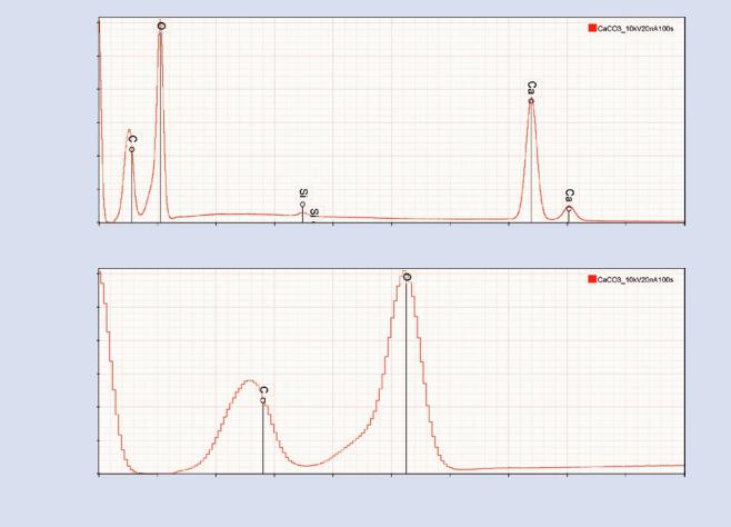
18 . Figure 18.1 shows an EDS spectrum for CaCO3 in which the O K peak at 0.523 keV is found at the correct energy, but the C K peak at 0.282 keV shows a significant deviation below the correct energy due to non-linear response in this range caused by incomplete charge collection.
All calibration spectra should be stored as part of the laboratory Quality Assurance documentation, and the calibration procedure should be performed regularly, preferably weekly and especially whenever the EDS system is powered down and restarted.
18.2\ Principles of Qualitative EDS Analysis
The knowledge base needed to accomplish high-confidence peak identification consists of three components: (1) the physics of characteristic X-ray generation and propagation; (2) a complete database of the energies of all critical ionization energies and corresponding characteristic peaks for all elements (except H and He, which do not produce characteristic X-rays); and (3) the artifacts inherent in EDS measurement.
18.2.1\ Critical Concepts From the Physics
of Characteristic X-ray Generation
and Propagation
What factors determine if characteristic peaks are generated and detectable?
Exciting Characteristic X-Rays
A specific characteristic X-ray can only be produced if the incident beam energy, E0, exceeds the critical ionization energy, Ec, for the atomic shell whose ionization leads to the emission of that characteristic X-ray. This requirement is parameterized as the overvoltage, U0:
U0 = E0 / Ec >1 \ |
(18.1) |
Note that for a particular element, if the beam energy is selected so that U0 > 1 for the K-shell, then for higher atomic number elements with complex atomic shell structures, shells with lower values of Ec will also be ionized; for example, if Cu K-shell X-rays are created, there will also be Cu L-shell X-rays, Au L-family, and Au M-family X-rays, etc.
While U0 > 1 sets the minimum beam energy criterion to generate a particular characteristic X-ray, the relative intensity of that X-ray generated from a thick target (where the thickness exceeds the electron range) depends on the overvoltage and the incident beam current, iB:
Ich ~ iB (U0 − 1)n \ |
(18.2) |
where the exponent n is approximately 1.5. The X-ray continuum intensity, Icm, that forms the spectral background at all photon energies up to E0 (the Duane–Hunt limit), arises from the electron bremsstrahlung and depends on the photon energy, Eν, and the beam energy:
Icm |
~ iB (E0 − Eν ) / Eν |
\ |
(18.3a) |
|
|
~ iB (U0 − 1) |
|
|
|
Icm |
for Eν ~ Ec \ |
(18.3b) |
||
18.2 · Principles of Qualitative EDS Analysis
|
120 000 |
|
O |
|
|
|
L-K |
|
100 000 |
|
|
|
80 000 |
C |
|
Counts |
|
-K |
|
60 000 |
L |
|
|
|
|
|
|
|
40 000 |
|
|
|
20 000 |
|
|
|
0 |
|
|
|
0.0 |
0.5 |
1.0 |
267 |
|
18 |
|
|
|
CaCO3 |
L-CaK |
E0 = 10 keV |
2,3 |
|
3M-CaK
1.5 |
2.0 |
2.5 |
3.0 |
3.5 |
4.0 |
4.5 |
5.0 |
|
Photon energy (keV) |
|
|
|
|
|
|
Counts
120 000
100 000
80 000
60 000
40 000
20 000
0
0.0
L-K C |
L-K O |
0.10 |
0.20 |
0.30 |
0.40 |
0.50 |
0.60 |
0.70 |
0.80 |
0.90 |
1.00 |
|
|
|
Photon energy (keV) |
|
|
|
|
||
. Fig. 18.1 Spectrum of calcium carbonate. Note non-linear behavior at low photon energy, e.g., the C K-shell peak is significantly shifted below the true energy value given by the marker
The characteristic peak to continuum background, P/B, which determines the visibility of peaks above the background, is found as the ratio of equations (18.2) and (18.3b):
P / B = Ich / Icm ~ (U0 − 1)n / (U0 − 1) |
|
|
= (U0 − 1)n −1 |
\ |
(18.4) |
|
|
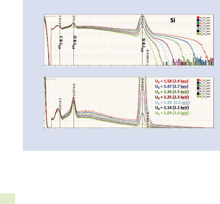
Since the exponent n ~ 1.5, in the expression for P/B the value of n − 1 ~ 0.5, so that as U0 is lowered, the P/B decreases dramatically, reducing the visibility of peaks, as shown in
. Fig. 18.2 for the K-shell peaks of silicon.
Fluorescence Yield
A second factor that affects the detectability of characteristic peaks is the fluorescence yield, the fraction of ionizations that leads to photon emission. The fluorescence yield varies sharply
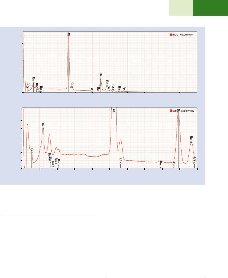
depending on the shells involved, with the fluorescence yields for a particular element generally trending K>L >>M. An example for barium L-shell and M-shell X-rays is shown in
. Fig. 18.3, where the Ba M-family X-rays are seen to have a much lower P/B than the Ba L-family X-rays, making Ba difficult to identify with high confidence if only the Ba M-family is excited, a condition that will exist for Ba if E0 is chosen below the 5.25 keV ionization energy for the Ba L3-shell.
X-ray Absorption
A third factor which can strongly influence the visibility and detection of peaks is absorption of characteristic X-rays as they travel through the specimen and the window and surface layers of the EDS detector. X-ray absorption along a path of length s through the specimen is a non-linear process:
|
0 |
( |
|
) |
|
|
|
I / I |
|
= exp − |
µ / ρ |
|
ρs |
\ |
(18.5) |
|
|
|
|
|
|
|
\268 Chapter 18 · Qualitative Elemental Analysis by Energy Dispersive X-Ray Spectrometry
Counts
Counts
10 000 |
|
|
|
|
|
|
|
|
|
|
|
|
|
|
|
1 000 |
|
|
|
|
|
|
|
|
|
|
|
|
|
|
|
100 |
|
|
|
|
|
|
|
|
|
|
|
|
|
|
|
10 |
|
|
|
|
|
|
|
|
|
|
|
|
|
|
|
1 |
0.2 |
0.4 |
0.6 |
0.8 |
1.0 |
1.2 |
1.4 |
1.6 |
1.8 |
2.0 |
2.2 |
2.4 |
2.6 |
2.8 |
3.0 |
0.0 |
|||||||||||||||
|
|
|
|
|
|
|
Photon energy (keV) |
|
|
|
|
|
|
||
14 000 |
|
|
|
|
|
|
|
|
|
|
|
|
|
|
|
12 000 |
|
|
|
|
|
|
|
|
|
|
|
|
|
|
|
10 000 |
|
|
|
|
|
|
|
|
|
|
|
|
|
|
|
8 000 |
|
|
|
|
|
|
|
|
|
|
|
|
|
|
|
6 000 |
|
|
|
|
|
|
|
|
|
|
|
|
|
|
|
4 000 |
|
|
|
|
|
|
|
|
|
|
|
|
|
|
|
2 000 |
|
|
|
|
|
|
|
|
|
|
|
|
|
|
|
0 |
0.2 |
0.4 |
0.6 |
0.8 |
1.0 |
1.2 |
1.4 |
1.6 |
1.8 |
2.0 |
2.2 |
2.4 |
2.6 |
2.8 |
3.0 |
0.0 |
|||||||||||||||
Photon energy (keV)
. Fig. 18.2 Si at various overvoltages, showing diminishing peak visibility as the excitation decreases
where I0 is the original intensity and I is the intensity that remains after path s through a material of density ρ having a mass absorption coefficient μ/ρ for the photon energy of interest. The mass absorption coefficient depends strongly on the photon energy and the specific elements that the photons are passing through. Generally, a photon will be strongly
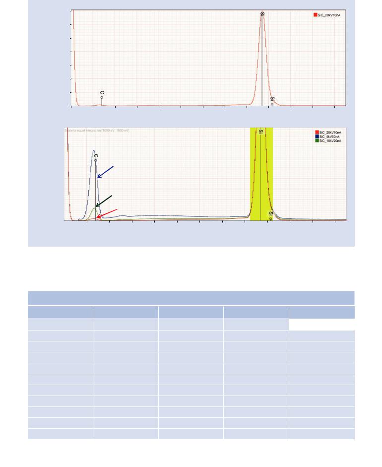
18 absorbed, i.e., there will be a large mass absorption coefficient, if the energy of the photon lies in a range of approximately 1 keV above the critical ionization energy for another element that is present in the analyzed volume. An extreme case is illustrated in . Fig. 18.4 for SiC, where at E0 = 20 keV with the spectrum scaled to the Si K-peak, the C K peak is barely visible despite C’s making up half of the composition on an atomic basis. Strong absorption of the C K X-ray at 0.282 keV occurs because this energy lies just above the Si L3 critical ionization energy at 0.110 keV, resulting in an extremely large value for the mass absorption coefficient. (There are also other factors that apply to this case, including the relative fluorescence yields, for which ωC < ωSi, and the
relative detector efficiency, εC < εSi, as described in the “EDS” module.) Because the absorption path length, s, depends strongly on the electron range, RK-O, which scales approximately as the 1.7 power of the incident beam energy, decreasing the beam energy reduces the absorption path of the C K X-rays, making the C K-peak more prominent relative to the Si K-peak, as shown in . Fig. 18.4 for a series of progressively lower beam energies.
The possibility of a high absorption situation for elements that must be measured with a low photon energy requires an analytical strategy such that when analyzing an unknown, the analyst should start at high beam energy, E0 ≥ 20 keV, and work down in beam energy. The analyst must be prepared to utilize low beam energies, E0 ≤ 5 keV, to evaluate the possibility of high absorption situations, such as those encountered for low atomic number elements (Z < 10). For these elements, the only detectable peaks have low photon energies (<1 keV) and are thus subject to high absorption when high incident beam energy is used.
269 |
18 |
18.2 · Principles of Qualitative EDS Analysis
Counts
Counts
140 000 |
|
|
|
|
|
|
|
|
|
|
120 000 |
|
|
|
|
|
BaCl2 |
(on C-substrate) |
|
|
|
|
|
|
|
|
|
|
|
|||
100 000 |
|
|
|
|
|
E0 = 10 keV |
|
|
|
|
|
|
|
|
|
|
|
|
|
|
|
80 000 |
|
|
|
|
|
|
|
|
|
|
60 000 |
|
|
|
|
|
|
|
|
|
|
40 000 |
|
|
|
|
|
|
|
|
|
|
20 000 |
|
|
|
|
|
|
|
|
|
|
0 |
|
|
|
|
|
|
|
|
|
|
0.0 |
1.0 |
2.0 |
3.0 |
4.0 |
5.0 |
6.0 |
7.0 |
8.0 |
9.0 |
10.0 |
|
|
|
|
|
Photon energy (keV) |
|
|
|
|
|
35 000 |
|
|
|
|
|
|
|
|
|
|
30 000 |
|
|
|
|
|
|
|
|
|
|
25 000 |
|
|
|
|
|
|
|
|
|
|
20 000 |
|
|
|
|
|
|
|
|
|
|
15 000 |
|
|
|
|
|
|
|
|
|
|
10 000 |
|
|
|
|
|
|
|
|
|
|
5 000 |
|
|
|
|
|
|
|
|
|
|
0 |
|
|
|
|
|
|
|
|
|
|
0.0 |
0.5 |
1.0 |
1.5 |
2.0 |
2.5 |
3.0 |
3.5 |
4.0 |
4.5 |
5.0 |
Photon energy (keV)
. Fig. 18.3 EDS spectrum of BaCl2 showing Ba L-family and Ba M-family peaks
18.2.2\ X-Ray Energy Database: Families
of X-Rays
The X-ray energy database is typically accessed through EDS software as a display of “KLM” markers showing the position of the peak (and possibly also the corresponding critical ionization energies) and the relative peak heights of the members of each X-ray family, examples of which are seen in . Figs. 18.1, 18.2, 18.3, and 18.4. The underlying database must contain such all characteristic X-rays (for ionization energies up to 25 keV) for all elements (excepting H and He which do not produce characteristic X-rays). No elements should be excluded, all X-ray families with photon energies below 30 keV should be included, and no minor X-ray family members should be excluded. As an example, a section of the DTSA-II X-ray energy database that displays the information for gold is presented in
. Table 18.1. While it is true that many of the closely spaced (in photon energy) and low abundance X-ray peaks cannot
be resolved by EDS because of the limited energy resolution, these peaks are nevertheless convolved in the measured spectrum. When a constituent is present at high concentration and is excited with adequate overvoltage, at least some of these low abundance family members will be readily
detectable, for example, the L3-M1 (Ll) and M4,5N2,3 (Mζ) peaks, as shown for Ba in . Fig. 18.5 and the AuM4,5N2,3, AuM1N1,3 and AuM2N4 peaks seen in . Fig. 18.6. Note also that the low energy performance of the silicon drift detec-
tor (SDD)-EDS is such that the Au N-family peaks are detected.
18.2.3\ Artifacts of the EDS Detection
Process
The EDS detection process is subject to two principal artifacts that must be properly cataloged to avoid subsequent misidentification.
\270 Chapter 18 · Qualitative Elemental Analysis by Energy Dispersive X-Ray Spectrometry
Counts
350 000 |
|
|
|
|
|
|
|
|
|
|
|
|
|
|
|
|
|
|
|
|
|
|
|
|
|
|
|
||
300 000 |
|
|
|
|
|
|
|
|
|
|
|
|
|
|
|
|
|
|
|
|
|
|
SiC |
|
|
|
|
|
|
250 000 |
|
|
|
|
|
|
E0 = 20 keV |
|
|
|
|
|
|
|
200 000 |
|
|
|
|
|
|
|
|
|
-SiK |
|
|
|
|
|
|
|
|
|
|
|
|
|
|
|
L |
|
|
|
150 000 |
|
|
|
|
|
|
|
|
|
2,3 |
|
|
|
|
|
|
|
|
|
|
|
|
|
|
|
|
|
||
100 000 |
|
|
-K C |
|
|
|
|
|
|
|
|
|
|
|
|
|
L |
|
|
|
|
|
|
|
|
|
|
||
|
|
|
|
|
|
|
|
|
|
|
|
|
|
|
50 000 |
|
|
|
|
|
|
|
|
|
|
|
|
|
|
0 |
|
|
|
|
|
|
|
|
|
|
|
|
|
|
|
|
|
|
|
|
|
|
|
|
|
|
|
||
0.0 |
0.2 |
0.4 |
0.6 |
0.8 |
1.0 |
1.2 |
1.4 |
1.6 |
1.8 |
2.0 |
2.2 |
2.4 |
||
|
|
|
|
|
|
|
|
Photon energy (keV) |
|
|
|
|
|
|
|
|
|
|
|
|
|
|
|
|
|
|
|
|
|
|
|
|
L-K C |
|
|
|
|
|
|
|
|
|
|
|
|
|
|
|
5 keV |
|
|
|
|
|
|
L-SiK |
|
|
|
|
|
|
|
|
|
|
|
|
|
|
|
|
|
|
|
|
|
|
|
|
|
|
|
|
|
2,3 |
|
|
|
|
|
|
|
10 keV |
|
|
|
|
|
|
|
|
|
|
|
|
|
|
20 keV |
|
|
|
|
|
|
|
|
|
|
|
|
|
|
|
|
|
|
|
|
|
|
|
|
|
0.0 |
|
0.2 |
0.4 |
0.6 |
0.8 |
1.0 |
1.2 |
1.4 |
1.6 |
1.8 |
2.0 |
2.2 |
2.4 |
|
|
|
|
|
|
|
|
|
Photon energy (keV) |
|
|
|
|
|
|
. Fig. 18.4 EDS spectra of SiC: (upper) at E0 = 20 keV, the C K-L3 peak is barely visible; (lower) as the beam energy is lowered to reduce absorption, the C K-L3 peak becomes more prominent (all spectra scaled to the Si K-L3 region.)
. Table 18.1 Comprehensive listing of all X-ray transitions for gold (DTSA-II database)
|
IUPAC |
Siegbahn |
Weight |
Energy (keV) |
Wavelength ( ) |
|
|
|
Au Kβ4 |
|
|
|
|
|
Au K-N5 |
0.0000 |
80.391 |
0.154226 |
||
18 |
||||||
Au K-N3 |
Au Kβ2 |
0.0500 |
80.1795 |
0.154633 |
||
|
||||||
|
||||||
|
Au K-M5 |
Au Kβ5 |
0.0005 |
78.5192 |
0.157903 |
|
|
Au K-M3 |
Au Kβ1 |
0.1500 |
77.9819 |
0.158991 |
|
|
Au K-M2 |
Au Kβ3 |
0.1500 |
77.5771 |
0.159821 |
|
|
Au K-L3 |
Au Kα1 |
1.0000 |
68.8062 |
0.180193 |
|
|
Au K-L2 |
Au Kα2 |
0.5000 |
66.9913 |
0.185075 |
|
|
Au L1-O4 |
Au L1O4/L1O5 |
0.0027 |
14.3445 |
0.864333 |
|
|
Au L1-O3 |
Au Lγ4 |
0.0062 |
14.2991 |
0.867077 |
|
|
Au L1-O2 |
Au Lγ4p |
0.0001 |
14.2811 |
0.86817 |
|
|
Au L1-O1 |
Au L1O1 |
0.0027 |
14.245 |
0.87037 |
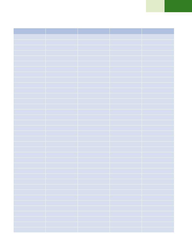
271 |
18 |
18.2 · Principles of Qualitative EDS Analysis
. Table 18.1 |
(continued) |
|
|
|
|
|
|
|
|
IUPAC |
Siegbahn |
Weight |
Energy (keV) |
Wavelength ( ) |
Au L1-N5 |
Au Lγ11 |
0.0007 |
14.0189 |
0.884407 |
Au L1-N4 |
Au L1N4 |
0.0001 |
14.0008 |
0.885551 |
Au L1-N3 |
Au Lγ3 |
0.0194 |
13.8074 |
0.897955 |
Au L2-O4 |
Au Lγ6 |
0.0109 |
13.7253 |
0.903326 |
Au L1-N2 |
Au Lγ2 |
0.0015 |
13.7091 |
0.904393 |
Au L2-O3 |
Au L2O3 |
0.0001 |
13.6799 |
0.906324 |
Au L2-O2 |
Au L2O2 |
0.0001 |
13.6619 |
0.907518 |
Au L2-N6 |
Au Lν |
0.0003 |
13.6472 |
0.908495 |
Au L2-O1 |
Au Lγ8 |
0.0007 |
13.6258 |
0.909922 |
Au L1-N1 |
Au L1N1 |
0.0001 |
13.594 |
0.912051 |
Au L2-N5 |
Au L2N5 |
0.0001 |
13.3997 |
0.925276 |
Au L2-N4 |
Au Lγ1 |
0.0841 |
13.3816 |
0.926527 |
Au L2-N3 |
Au L2N3 |
0.0027 |
13.1882 |
0.940115 |
Au L2-N2 |
Au L2N2 |
0.0001 |
13.0899 |
0.947174 |
Au L2-N1 |
Au Lγ5 |
0.0035 |
12.9748 |
0.955577 |
Au L1-M5 |
Au Lβ9 |
0.0004 |
12.1471 |
1.02069 |
Au L1-M4 |
Au Lβ10 |
0.0054 |
12.0617 |
1.02792 |
Au L3-P1 |
Au L3P1 |
0.0001 |
11.935 |
1.03883 |
Au L3-O4 |
Au Lβ5 |
0.0438 |
11.9104 |
1.04097 |
Au L3-O2 |
Au L3O2 |
0.0001 |
11.847 |
1.04655 |
Au L3-N6 |
Au Lu |
0.0009 |
11.8323 |
1.04785 |
Au L3-O1 |
Au Lβ7 |
0.0004 |
11.8109 |
1.04974 |
Au L1-M3 |
Au Lβ3 |
0.0690 |
11.6098 |
1.06793 |
Au L3-N5 |
Au Lβ2 |
0.2195 |
11.5848 |
1.07023 |
Au L3-N4 |
Au Lβ15 |
0.0000 |
11.5667 |
1.07191 |
Au L2-M5 |
Au L2M5 |
0.0001 |
11.5279 |
1.07551 |
Au L2-M4 |
Au Lβ1 |
0.4015 |
11.4425 |
1.08354 |
Au L3-N3 |
Au L3N3 |
0.0001 |
11.3733 |
1.09013 |
Au L3-N2 |
Au L3N2 |
0.0001 |
11.275 |
1.09964 |
Au L1-M2 |
Au Lβ4 |
0.0594 |
11.205 |
1.10651 |
Au L3-N1 |
Au Lβ6 |
0.0140 |
11.1599 |
1.11098 |
Au L2-M3 |
Au Lβ17 |
0.0005 |
10.9906 |
1.12809 |
Au L1-M1 |
Au L1M1 |
0.0001 |
10.9279 |
1.13457 |
Au L2-M2 |
Au L2M2 |
0.0001 |
10.5858 |
1.17123 |
Au L2-M1 |
Au Lη |
0.0138 |
10.3087 |
1.20271 |
Au L3-M5 |
Au Lα1 |
1.0000 |
9.713 |
1.27648 |
Au L3-M4 |
Au Lα2 |
0.1139 |
9.6276 |
1.2878 |
(continued)