

- •Preface
- •Imaging Microscopic Features
- •Measuring the Crystal Structure
- •References
- •Contents
- •1.4 Simulating the Effects of Elastic Scattering: Monte Carlo Calculations
- •What Are the Main Features of the Beam Electron Interaction Volume?
- •How Does the Interaction Volume Change with Composition?
- •How Does the Interaction Volume Change with Incident Beam Energy?
- •How Does the Interaction Volume Change with Specimen Tilt?
- •1.5 A Range Equation To Estimate the Size of the Interaction Volume
- •References
- •2: Backscattered Electrons
- •2.1 Origin
- •2.2.1 BSE Response to Specimen Composition (η vs. Atomic Number, Z)
- •SEM Image Contrast with BSE: “Atomic Number Contrast”
- •SEM Image Contrast: “BSE Topographic Contrast—Number Effects”
- •2.2.3 Angular Distribution of Backscattering
- •Beam Incident at an Acute Angle to the Specimen Surface (Specimen Tilt > 0°)
- •SEM Image Contrast: “BSE Topographic Contrast—Trajectory Effects”
- •2.2.4 Spatial Distribution of Backscattering
- •Depth Distribution of Backscattering
- •Radial Distribution of Backscattered Electrons
- •2.3 Summary
- •References
- •3: Secondary Electrons
- •3.1 Origin
- •3.2 Energy Distribution
- •3.3 Escape Depth of Secondary Electrons
- •3.8 Spatial Characteristics of Secondary Electrons
- •References
- •4: X-Rays
- •4.1 Overview
- •4.2 Characteristic X-Rays
- •4.2.1 Origin
- •4.2.2 Fluorescence Yield
- •4.2.3 X-Ray Families
- •4.2.4 X-Ray Nomenclature
- •4.2.6 Characteristic X-Ray Intensity
- •Isolated Atoms
- •X-Ray Production in Thin Foils
- •X-Ray Intensity Emitted from Thick, Solid Specimens
- •4.3 X-Ray Continuum (bremsstrahlung)
- •4.3.1 X-Ray Continuum Intensity
- •4.3.3 Range of X-ray Production
- •4.4 X-Ray Absorption
- •4.5 X-Ray Fluorescence
- •References
- •5.1 Electron Beam Parameters
- •5.2 Electron Optical Parameters
- •5.2.1 Beam Energy
- •Landing Energy
- •5.2.2 Beam Diameter
- •5.2.3 Beam Current
- •5.2.4 Beam Current Density
- •5.2.5 Beam Convergence Angle, α
- •5.2.6 Beam Solid Angle
- •5.2.7 Electron Optical Brightness, β
- •Brightness Equation
- •5.2.8 Focus
- •Astigmatism
- •5.3 SEM Imaging Modes
- •5.3.1 High Depth-of-Field Mode
- •5.3.2 High-Current Mode
- •5.3.3 Resolution Mode
- •5.3.4 Low-Voltage Mode
- •5.4 Electron Detectors
- •5.4.1 Important Properties of BSE and SE for Detector Design and Operation
- •Abundance
- •Angular Distribution
- •Kinetic Energy Response
- •5.4.2 Detector Characteristics
- •Angular Measures for Electron Detectors
- •Elevation (Take-Off) Angle, ψ, and Azimuthal Angle, ζ
- •Solid Angle, Ω
- •Energy Response
- •Bandwidth
- •5.4.3 Common Types of Electron Detectors
- •Backscattered Electrons
- •Passive Detectors
- •Scintillation Detectors
- •Semiconductor BSE Detectors
- •5.4.4 Secondary Electron Detectors
- •Everhart–Thornley Detector
- •Through-the-Lens (TTL) Electron Detectors
- •TTL SE Detector
- •TTL BSE Detector
- •Measuring the DQE: BSE Semiconductor Detector
- •References
- •6: Image Formation
- •6.1 Image Construction by Scanning Action
- •6.2 Magnification
- •6.3 Making Dimensional Measurements With the SEM: How Big Is That Feature?
- •Using a Calibrated Structure in ImageJ-Fiji
- •6.4 Image Defects
- •6.4.1 Projection Distortion (Foreshortening)
- •6.4.2 Image Defocusing (Blurring)
- •6.5 Making Measurements on Surfaces With Arbitrary Topography: Stereomicroscopy
- •6.5.1 Qualitative Stereomicroscopy
- •Fixed beam, Specimen Position Altered
- •Fixed Specimen, Beam Incidence Angle Changed
- •6.5.2 Quantitative Stereomicroscopy
- •Measuring a Simple Vertical Displacement
- •References
- •7: SEM Image Interpretation
- •7.1 Information in SEM Images
- •7.2.2 Calculating Atomic Number Contrast
- •Establishing a Robust Light-Optical Analogy
- •Getting It Wrong: Breaking the Light-Optical Analogy of the Everhart–Thornley (Positive Bias) Detector
- •Deconstructing the SEM/E–T Image of Topography
- •SUM Mode (A + B)
- •DIFFERENCE Mode (A−B)
- •References
- •References
- •9: Image Defects
- •9.1 Charging
- •9.1.1 What Is Specimen Charging?
- •9.1.3 Techniques to Control Charging Artifacts (High Vacuum Instruments)
- •Observing Uncoated Specimens
- •Coating an Insulating Specimen for Charge Dissipation
- •Choosing the Coating for Imaging Morphology
- •9.2 Radiation Damage
- •9.3 Contamination
- •References
- •10: High Resolution Imaging
- •10.2 Instrumentation Considerations
- •10.4.1 SE Range Effects Produce Bright Edges (Isolated Edges)
- •10.4.4 Too Much of a Good Thing: The Bright Edge Effect Hinders Locating the True Position of an Edge for Critical Dimension Metrology
- •10.5.1 Beam Energy Strategies
- •Low Beam Energy Strategy
- •High Beam Energy Strategy
- •Making More SE1: Apply a Thin High-δ Metal Coating
- •Making Fewer BSEs, SE2, and SE3 by Eliminating Bulk Scattering From the Substrate
- •10.6 Factors That Hinder Achieving High Resolution
- •10.6.2 Pathological Specimen Behavior
- •Contamination
- •Instabilities
- •References
- •11: Low Beam Energy SEM
- •11.3 Selecting the Beam Energy to Control the Spatial Sampling of Imaging Signals
- •11.3.1 Low Beam Energy for High Lateral Resolution SEM
- •11.3.2 Low Beam Energy for High Depth Resolution SEM
- •11.3.3 Extremely Low Beam Energy Imaging
- •References
- •12.1.1 Stable Electron Source Operation
- •12.1.2 Maintaining Beam Integrity
- •12.1.4 Minimizing Contamination
- •12.3.1 Control of Specimen Charging
- •12.5 VPSEM Image Resolution
- •References
- •13: ImageJ and Fiji
- •13.1 The ImageJ Universe
- •13.2 Fiji
- •13.3 Plugins
- •13.4 Where to Learn More
- •References
- •14: SEM Imaging Checklist
- •14.1.1 Conducting or Semiconducting Specimens
- •14.1.2 Insulating Specimens
- •14.2 Electron Signals Available
- •14.2.1 Beam Electron Range
- •14.2.2 Backscattered Electrons
- •14.2.3 Secondary Electrons
- •14.3 Selecting the Electron Detector
- •14.3.2 Backscattered Electron Detectors
- •14.3.3 “Through-the-Lens” Detectors
- •14.4 Selecting the Beam Energy for SEM Imaging
- •14.4.4 High Resolution SEM Imaging
- •Strategy 1
- •Strategy 2
- •14.5 Selecting the Beam Current
- •14.5.1 High Resolution Imaging
- •14.5.2 Low Contrast Features Require High Beam Current and/or Long Frame Time to Establish Visibility
- •14.6 Image Presentation
- •14.6.1 “Live” Display Adjustments
- •14.6.2 Post-Collection Processing
- •14.7 Image Interpretation
- •14.7.1 Observer’s Point of View
- •14.7.3 Contrast Encoding
- •14.8.1 VPSEM Advantages
- •14.8.2 VPSEM Disadvantages
- •15: SEM Case Studies
- •15.1 Case Study: How High Is That Feature Relative to Another?
- •15.2 Revealing Shallow Surface Relief
- •16.1.2 Minor Artifacts: The Si-Escape Peak
- •16.1.3 Minor Artifacts: Coincidence Peaks
- •16.1.4 Minor Artifacts: Si Absorption Edge and Si Internal Fluorescence Peak
- •16.2 “Best Practices” for Electron-Excited EDS Operation
- •16.2.1 Operation of the EDS System
- •Choosing the EDS Time Constant (Resolution and Throughput)
- •Choosing the Solid Angle of the EDS
- •Selecting a Beam Current for an Acceptable Level of System Dead-Time
- •16.3.1 Detector Geometry
- •16.3.2 Process Time
- •16.3.3 Optimal Working Distance
- •16.3.4 Detector Orientation
- •16.3.5 Count Rate Linearity
- •16.3.6 Energy Calibration Linearity
- •16.3.7 Other Items
- •16.3.8 Setting Up a Quality Control Program
- •Using the QC Tools Within DTSA-II
- •Creating a QC Project
- •Linearity of Output Count Rate with Live-Time Dose
- •Resolution and Peak Position Stability with Count Rate
- •Solid Angle for Low X-ray Flux
- •Maximizing Throughput at Moderate Resolution
- •References
- •17: DTSA-II EDS Software
- •17.1 Getting Started With NIST DTSA-II
- •17.1.1 Motivation
- •17.1.2 Platform
- •17.1.3 Overview
- •17.1.4 Design
- •Simulation
- •Quantification
- •Experiment Design
- •Modeled Detectors (. Fig. 17.1)
- •Window Type (. Fig. 17.2)
- •The Optimal Working Distance (. Figs. 17.3 and 17.4)
- •Elevation Angle
- •Sample-to-Detector Distance
- •Detector Area
- •Crystal Thickness
- •Number of Channels, Energy Scale, and Zero Offset
- •Resolution at Mn Kα (Approximate)
- •Azimuthal Angle
- •Gold Layer, Aluminum Layer, Nickel Layer
- •Dead Layer
- •Zero Strobe Discriminator (. Figs. 17.7 and 17.8)
- •Material Editor Dialog (. Figs. 17.9, 17.10, 17.11, 17.12, 17.13, and 17.14)
- •17.2.1 Introduction
- •17.2.2 Monte Carlo Simulation
- •17.2.4 Optional Tables
- •References
- •18: Qualitative Elemental Analysis by Energy Dispersive X-Ray Spectrometry
- •18.1 Quality Assurance Issues for Qualitative Analysis: EDS Calibration
- •18.2 Principles of Qualitative EDS Analysis
- •Exciting Characteristic X-Rays
- •Fluorescence Yield
- •X-ray Absorption
- •Si Escape Peak
- •Coincidence Peaks
- •18.3 Performing Manual Qualitative Analysis
- •Beam Energy
- •Choosing the EDS Resolution (Detector Time Constant)
- •Obtaining Adequate Counts
- •18.4.1 Employ the Available Software Tools
- •18.4.3 Lower Photon Energy Region
- •18.4.5 Checking Your Work
- •18.5 A Worked Example of Manual Peak Identification
- •References
- •19.1 What Is a k-ratio?
- •19.3 Sets of k-ratios
- •19.5 The Analytical Total
- •19.6 Normalization
- •19.7.1 Oxygen by Assumed Stoichiometry
- •19.7.3 Element by Difference
- •19.8 Ways of Reporting Composition
- •19.8.1 Mass Fraction
- •19.8.2 Atomic Fraction
- •19.8.3 Stoichiometry
- •19.8.4 Oxide Fractions
- •Example Calculations
- •19.9 The Accuracy of Quantitative Electron-Excited X-ray Microanalysis
- •19.9.1 Standards-Based k-ratio Protocol
- •19.9.2 “Standardless Analysis”
- •19.10 Appendix
- •19.10.1 The Need for Matrix Corrections To Achieve Quantitative Analysis
- •19.10.2 The Physical Origin of Matrix Effects
- •19.10.3 ZAF Factors in Microanalysis
- •X-ray Generation With Depth, φ(ρz)
- •X-ray Absorption Effect, A
- •X-ray Fluorescence, F
- •References
- •20.2 Instrumentation Requirements
- •20.2.1 Choosing the EDS Parameters
- •EDS Spectrum Channel Energy Width and Spectrum Energy Span
- •EDS Time Constant (Resolution and Throughput)
- •EDS Calibration
- •EDS Solid Angle
- •20.2.2 Choosing the Beam Energy, E0
- •20.2.3 Measuring the Beam Current
- •20.2.4 Choosing the Beam Current
- •Optimizing Analysis Strategy
- •20.3.4 Ba-Ti Interference in BaTiSi3O9
- •20.4 The Need for an Iterative Qualitative and Quantitative Analysis Strategy
- •20.4.2 Analysis of a Stainless Steel
- •20.5 Is the Specimen Homogeneous?
- •20.6 Beam-Sensitive Specimens
- •20.6.1 Alkali Element Migration
- •20.6.2 Materials Subject to Mass Loss During Electron Bombardment—the Marshall-Hall Method
- •Thin Section Analysis
- •Bulk Biological and Organic Specimens
- •References
- •21: Trace Analysis by SEM/EDS
- •21.1 Limits of Detection for SEM/EDS Microanalysis
- •21.2.1 Estimating CDL from a Trace or Minor Constituent from Measuring a Known Standard
- •21.2.2 Estimating CDL After Determination of a Minor or Trace Constituent with Severe Peak Interference from a Major Constituent
- •21.3 Measurements of Trace Constituents by Electron-Excited Energy Dispersive X-ray Spectrometry
- •The Inevitable Physics of Remote Excitation Within the Specimen: Secondary Fluorescence Beyond the Electron Interaction Volume
- •Simulation of Long-Range Secondary X-ray Fluorescence
- •NIST DTSA II Simulation: Vertical Interface Between Two Regions of Different Composition in a Flat Bulk Target
- •NIST DTSA II Simulation: Cubic Particle Embedded in a Bulk Matrix
- •21.5 Summary
- •References
- •22.1.2 Low Beam Energy Analysis Range
- •22.2 Advantage of Low Beam Energy X-Ray Microanalysis
- •22.2.1 Improved Spatial Resolution
- •22.3 Challenges and Limitations of Low Beam Energy X-Ray Microanalysis
- •22.3.1 Reduced Access to Elements
- •22.3.3 At Low Beam Energy, Almost Everything Is Found To Be Layered
- •Analysis of Surface Contamination
- •References
- •23: Analysis of Specimens with Special Geometry: Irregular Bulk Objects and Particles
- •23.2.1 No Chemical Etching
- •23.3 Consequences of Attempting Analysis of Bulk Materials With Rough Surfaces
- •23.4.1 The Raw Analytical Total
- •23.4.2 The Shape of the EDS Spectrum
- •23.5 Best Practices for Analysis of Rough Bulk Samples
- •23.6 Particle Analysis
- •Particle Sample Preparation: Bulk Substrate
- •The Importance of Beam Placement
- •Overscanning
- •“Particle Mass Effect”
- •“Particle Absorption Effect”
- •The Analytical Total Reveals the Impact of Particle Effects
- •Does Overscanning Help?
- •23.6.6 Peak-to-Background (P/B) Method
- •Specimen Geometry Severely Affects the k-ratio, but Not the P/B
- •Using the P/B Correspondence
- •23.7 Summary
- •References
- •24: Compositional Mapping
- •24.2 X-Ray Spectrum Imaging
- •24.2.1 Utilizing XSI Datacubes
- •24.2.2 Derived Spectra
- •SUM Spectrum
- •MAXIMUM PIXEL Spectrum
- •24.3 Quantitative Compositional Mapping
- •24.4 Strategy for XSI Elemental Mapping Data Collection
- •24.4.1 Choosing the EDS Dead-Time
- •24.4.2 Choosing the Pixel Density
- •24.4.3 Choosing the Pixel Dwell Time
- •“Flash Mapping”
- •High Count Mapping
- •References
- •25.1 Gas Scattering Effects in the VPSEM
- •25.1.1 Why Doesn’t the EDS Collimator Exclude the Remote Skirt X-Rays?
- •25.2 What Can Be Done To Minimize gas Scattering in VPSEM?
- •25.2.2 Favorable Sample Characteristics
- •Particle Analysis
- •25.2.3 Unfavorable Sample Characteristics
- •References
- •26.1 Instrumentation
- •26.1.2 EDS Detector
- •26.1.3 Probe Current Measurement Device
- •Direct Measurement: Using a Faraday Cup and Picoammeter
- •A Faraday Cup
- •Electrically Isolated Stage
- •Indirect Measurement: Using a Calibration Spectrum
- •26.1.4 Conductive Coating
- •26.2 Sample Preparation
- •26.2.1 Standard Materials
- •26.2.2 Peak Reference Materials
- •26.3 Initial Set-Up
- •26.3.1 Calibrating the EDS Detector
- •Selecting a Pulse Process Time Constant
- •Energy Calibration
- •Quality Control
- •Sample Orientation
- •Detector Position
- •Probe Current
- •26.4 Collecting Data
- •26.4.1 Exploratory Spectrum
- •26.4.2 Experiment Optimization
- •26.4.3 Selecting Standards
- •26.4.4 Reference Spectra
- •26.4.5 Collecting Standards
- •26.4.6 Collecting Peak-Fitting References
- •26.5 Data Analysis
- •26.5.2 Quantification
- •26.6 Quality Check
- •Reference
- •27.2 Case Study: Aluminum Wire Failures in Residential Wiring
- •References
- •28: Cathodoluminescence
- •28.1 Origin
- •28.2 Measuring Cathodoluminescence
- •28.3 Applications of CL
- •28.3.1 Geology
- •Carbonado Diamond
- •Ancient Impact Zircons
- •28.3.2 Materials Science
- •Semiconductors
- •Lead-Acid Battery Plate Reactions
- •28.3.3 Organic Compounds
- •References
- •29.1.1 Single Crystals
- •29.1.2 Polycrystalline Materials
- •29.1.3 Conditions for Detecting Electron Channeling Contrast
- •Specimen Preparation
- •Instrument Conditions
- •29.2.1 Origin of EBSD Patterns
- •29.2.2 Cameras for EBSD Pattern Detection
- •29.2.3 EBSD Spatial Resolution
- •29.2.5 Steps in Typical EBSD Measurements
- •Sample Preparation for EBSD
- •Align Sample in the SEM
- •Check for EBSD Patterns
- •Adjust SEM and Select EBSD Map Parameters
- •Run the Automated Map
- •29.2.6 Display of the Acquired Data
- •29.2.7 Other Map Components
- •29.2.10 Application Example
- •Application of EBSD To Understand Meteorite Formation
- •29.2.11 Summary
- •Specimen Considerations
- •EBSD Detector
- •Selection of Candidate Crystallographic Phases
- •Microscope Operating Conditions and Pattern Optimization
- •Selection of EBSD Acquisition Parameters
- •Collect the Orientation Map
- •References
- •30.1 Introduction
- •30.2 Ion–Solid Interactions
- •30.3 Focused Ion Beam Systems
- •30.5 Preparation of Samples for SEM
- •30.5.1 Cross-Section Preparation
- •30.5.2 FIB Sample Preparation for 3D Techniques and Imaging
- •30.6 Summary
- •References
- •31: Ion Beam Microscopy
- •31.1 What Is So Useful About Ions?
- •31.2 Generating Ion Beams
- •31.3 Signal Generation in the HIM
- •31.5 Patterning with Ion Beams
- •31.7 Chemical Microanalysis with Ion Beams
- •References
- •Appendix
- •A Database of Electron–Solid Interactions
- •A Database of Electron–Solid Interactions
- •Introduction
- •Backscattered Electrons
- •Secondary Yields
- •Stopping Powers
- •X-ray Ionization Cross Sections
- •Conclusions
- •References
- •Index
- •Reference List
- •Index
172\ Chapter 11 · Low Beam Energy SEM
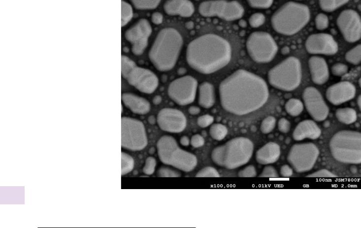
. Fig. 11.8 Extremely low landing energy (E0 = 0.010 keV) image of gold islands evaporated on carbon; TTL SE detector;
Bar = 100 nm (Image courtesy of V. Robertson, JEOL)
11
References
Bongeler R, Golla U, Kussens M, Reimer L, Schendler B, Senkel R, Spranck M (1993) Electron-specimen interactions in low-voltage scanning electron microscopy. Scanning 15:1
Bronstein IM, Fraiman BS (1969) “Secondary electron emission” Vtorichnaya elektronnaya emissiya. Nauka, Moskva, p 340
Bruining H, De Boer JM (1938) Secondary electron emission: Part 1 secondary electron emission of metals. Phys Ther 5:17p
Hilleret N, Bojko J, Grobner O, Henrist B, Scheuerlein C, and Taborelli M (2000) “The secondary electron yield of technical materials and its Variation with surface treatments” in Proc.7th European Particle Accelerator Conference, Vienna
Joy D (2012) Can be found in chapter 3 on SpringerLink: http://link. springer.com/chapter/10.1007/978-1-4939-6676-9_3
Kanter M (1961) Energy dissipation and secondary electron emission in solids. Phys Rev 121:1677
Moncrieff DA, Barker PR (1976) Secondary electron emission in the scanning electron microscope. Scanning 1:195
Reimer L, Tolkamp C (1980) Measuring the backscattering coefficient and secondary electron yield inside a scanning electron microscope. Scanning 3:35
Shimizu R (1974) Secondary electron yield with primary electron beam of keV. J Appl Phys 45:2107
173 |
|
12 |
|
|
|
Variable Pressure Scanning
Electron Microscopy (VPSEM)
12.1\ Review: The Conventional SEM High Vacuum
Environment – 174
12.1.1\ Stable Electron Source Operation – 174
12.1.2\ Maintaining Beam Integrity – 174
12.1.3\ Stable Operation of the Everhart–Thornley Secondary
Electron Detector – 174
12.1.4\ Minimizing Contamination – 174
12.2\ How Does VPSEM Differ From the Conventional
SEM Vacuum Environment? – 174
12.3\ Benefits of Scanning Electron Microscopy at
Elevated Pressures – 175
12.3.1\ Control of Specimen Charging – 175
12.3.2\ Controlling the Water Environment of a Specimen – 176
12.4\ Gas Scattering Modification of the Focused
Electron Beam – 177
12.5\ VPSEM Image Resolution – 181
12.6\ Detectors for Elevated Pressure Microscopy – 182
12.6.1\ Backscattered Electrons—Passive Scintillator Detector – 182 12.6.2\ Secondary Electrons–Gas Amplification Detector – 182
12.7\ Contrast in VPSEM – 184
\References – 185
© Springer Science+Business Media LLC 2018
J. Goldstein et al., Scanning Electron Microscopy and X-Ray Microanalysis, https://doi.org/10.1007/978-1-4939-6676-9_12

\174 Chapter 12 · Variable Pressure Scanning Electron Microscopy (VPSEM)
12.1\ Review: The Conventional SEM High
Vacuum Environment
The conventional SEM must operate with a pressure in the sample chamber below ~10−4 Pa (~10−6 torr), a condition determined by the need to satisfy four key instrumental operating conditions:
12.1.1\ Stable Electron Source Operation
The pressure in the electron gun must be maintained below 10−4 Pa (~10−6 torr) for stable operation of a conventional thermal emission tungsten filament and below 10−7 Pa (~10−9 torr) for a thermally assisted field emission source. Although a separate pumping system is typically devoted to the electron source to maintain the proper vacuum, if the specimen chamber pressure in a conventional SEM is allowed to rise, gas molecules will diffuse to the gun, raising the pressure and causing unstable operation and early failure.
12.1.2\ Maintaining Beam Integrity
An electron emitted from the source that encounters a gas atom along the path to the specimen will scatter elastically, changing the trajectory and causing the electron to deviate
12 out of the focused beam. To preserve the integrity of the beam, the column and chamber pressure must be reduced to the point that the number of collisions between the beam electrons and the residual gas molecules is negligible along the entire path, which typically extends to 25 cm or more.
12.1.3\ Stable Operation of the Everhart–
Thornley Secondary Electron
Detector
To serve as a detector for secondary electrons, the Everhart– Thornley secondary electron detector must be operated with a bias of +10,000 volts or more applied to the face of the scintillator to accelerate the SE and raise their kinetic energy sufficiently to cause light emission. If the chamber pressure exceeds approximately 100 mPa (~10−3 torr), electrical discharge events will begin to occur due to gas ionization between the scintillator (+10,000 V) and the Faraday cage (+250 V), which is located in close proximity, initially increasing the noise and thus degrading the signal-to-noise ratio. As the chamber pressure is further increased, electrical arcing will eventually cause total operational failure.
12.1.4\ Minimizing Contamination
A major source of specimen contamination during examination arises from the cracking of hydrocarbons by the electron
beam. A critical factor in determining contamination rates is the availability of hydrocarbon molecules for the beam electrons to hit. To achieve a low contamination environment, the pumping system must be capable of achieving low ultimate operating pressures. A specimen exchange airlock can pump off most volatiles, minimizing the exposure of the specimen chamber, and the airlock can be augmented with a plasma cleaning system to actively destroy volatiles. Finally, the vacuum system can be augmented with careful cold surface trapping of any remaining volatiles from the specimen or those that can backstream from the pump so as to minimize the partial pressure of hydrocarbons. Most importantly, to avoid introducing unnecessary sources of contamination, the microscopist must be very careful in handling instrument parts and specimens to avoid inadvertently depositing highly volatile hydrocarbons, such as those associated with skin oils deposited in fingerprints, into the conventional
SEM. With this level of operational care when operating in a well maintained modern instrument, beam-induced contamination when observed almost always results from residual hydrocarbons on the specimen which remain from incomplete cleaning rather than from hydrocarbons from the vacuum system itself.
A significant price is paid to operate the SEM with such a “clean” high vacuum. The specimen must be prepared in a condition so as not to evolve gases in the vacuum environment. Many important materials, such as biological tissues, contain liquid water, which will rapidly evaporate at reduced pressure, distorting the microscopic details of a specimen and disturbing the stable operating conditions of the microscope. This water, and any other volatile substances, must be removed during sample preparation to examine the specimen in a “dry” state, or the water must be immobilized by freezing to low temperatures (“frozen, hydrated samples”). Such specimen preparation is both time-consuming and prone to introducing artifacts, including the redistribution of “diffusible” elements, such as the alkali ions of salts.
12.2\ How Does VPSEM Differ
From the Conventional SEM Vacuum
Environment?
The development of the variable pressure scanning electron microscope (VPSEM) has enabled operation with elevated specimen chamber pressures in the range ~1–2500 Pa (~0.01–20 torr) while still maintaining a high level of SEM imaging performance (Danilatos 1988, 1991). The VPSEM utilizes “differential pumping” with several stages to obtain the desired elevated pressure in the specimen chamber while simultaneously maintaining a satisfactory pressure for stable operation of the electron gun and protection of the beam electrons from encountering elevated gas pressure along most of the flight path down the column.
Differential pumping consists of establishing a series of
12.3 · Benefits of Scanning Electron Microscopy at Elevated Pressures
regions of successively lower pressure, with each region separated by small apertures from the regions on either side and each region having its own dedicated pumping path. The probability of gas molecules moving from one region to the next is limited by the area of the aperture. In the VPSEM, these differential pumping apertures also serve as the beam-defining apertures. A typical vacuum design consists of separate pumping systems for the specimen chamber, one region for each lens, and finally the electron gun. Such a vacuum system can maintain a pressure differential of six orders of magnitude or more between the specimen chamber and the electron gun, enabling use of both conventional thermionic sources and thermally-assisted field emission sources. A wide variety of gases can be used in the elevated pressure sample chamber, including oxygen, nitrogen, argon, and water vapor. Because the imaging conditions are extremely sensitive to the sample chamber pressure, careful regulation of the pressure and of its stability for extended periods is required.
12.3\ Benefits of Scanning Electron
Microscopy at Elevated Pressures
There are several special benefits to performing scanning electron microscopy at elevated pressures.
12.3.1\ Control of Specimen Charging
Insulating materials suffer charging in the conventional high vacuum SEM because the high resistivity of the specimen prevents the migration of the charges injected by the beam, as partially offset by charges that leave the specimen as backscattered and secondary electrons, to reach an electrical ground. Consequently, there develops a local accumulation of charge. Depending on the beam energy, the material properties, and the local inclination of the specimen to the beam, negative or positive charging can occur. Charging phenomena can be manifest in many ways in SEM images, ranging at the threshold from diminished collection of secondary electrons which reduces the signal-to-noise ratio to more extreme effects where the local charge accumulation is high enough to cause actual displacement of the position of the beam, often seen as discontinuities in the scanned image. In the most extreme cases, the charge may be sufficient for the specimen to act as a mirror and deflect the beam entirely. In conventional SEM operation, charging is typically eliminated or at least minimized by applying a thin conducting coating to an insulating specimen and connecting the coating layer to electrical ground.
In the VPSEM, incident beam electrons, BSE and SE can scatter inelastically with gas atoms near the specimen, ionizing those gas atoms to create free low kinetic energy electrons and positive ions. Areas of an insulating specimen that charge will attract the appropriate oppo-
175 |
|
12 |
|
|
|
20 µm
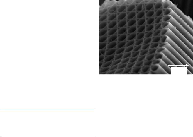
. Fig. 12.1 Uncoated glass polycapillary as imaged in a VPSEM (conditions: 20 keV; 500 Pa water vapor; gaseous secondary electron detector)
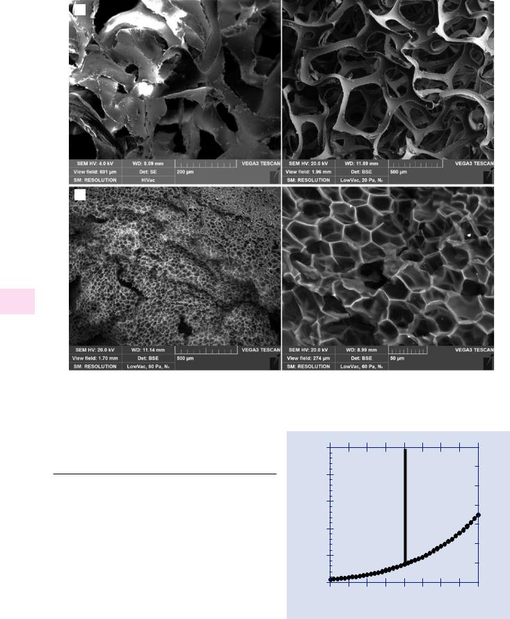
sitely charged species from this charge cloud, the positively ionized gas atoms or the free electrons, leading to local dynamic charge neutralization, enabling insulating materials to be examined without a coating. Moreover, the environmental gas, the ionized gas atoms, and the free electrons can penetrate into complex geometric features such as deep holes, features which would be very difficult to coat to establish a conducting path for conventional high vacuum SEM. An example of VPSEM imaging of a very complex insulating object is shown in . Fig. 12.1, which is an array of glass microcapillaries examined without any coating. No charging is observed in this secondary electron VPSEM image with E0 = 20 keV (prepared with a gaseous secondary electron detector, as described below) despite the very deep recesses in the structure. Another example is shown in . Fig. 12.2a, which shows a comparison of images of a complex polymer foam imaged in high vacuum SEM at a low beam energy of E0 = 4 keV with an Everhart–Thornley (E–T) detector, showing the development of charging, and in VPSEM mode with E0 = 20 keV and an off-axis backscattered electron (BSE) detector, showing no charging effects. A challenging insulating sample with a complex surface is shown in . Fig. 12.2b, which depicts fresh popcorn imaged under VPSEM conditions with a BSE detector.
Achieving suppression of charging for such complex insulating objects as those shown in . Figs. 12.1 and 12.2 involves careful control of the usual parameters of beam energy, beam current, and specimen tilt. In VPSEM operation the additional critical variables of environmental gas species and partial pressure must be carefully explored. Additionally, the special detectors for SE that have been developed for VPSEM operation can also play a role in charge suppression.
\176 Chapter 12 · Variable Pressure Scanning Electron Microscopy (VPSEM)
a
b
12
. Fig. 12.2 a Uncoated polymer foam imaged (left) with high vacuum SEM, E0 =4 keV, E-T(+) detector (bar = 200 µm); and (right) VPSEM, E0 =20 keV, off-axis BSE detector (bar = 500 µm) (Images courtesy
J. Mershan, TESCAN). b (left and right) Uncoated freshly popped popcorn
imaged with VPSEM, E0 =20 keV, BSE detector; 60 Pa N2 (left, bar = 500 µm) (right, bar = 50 µm) (Images courtesy J. Mershon, TESCAN; sample source: Lehigh Microscopy School)
12.3.2\ Controlling the Water Environment
of a Specimen
Careful control and preservation of the water content of a specimen can be critical to recording SEM images that are free from artifacts or suffer only minimal artifacts. Additionally, when there is control of the partial pressure of water vapor in the specimen chamber to maintain liquid water in equilibrium with the gas phase, it becomes possible to observe chemical reactions that are mediated by water.
By monitoring and controlling the relative humidity, it is possible to add water by condensation or remove it by evaporation. . Figure 12.3 shows the pressure–tempera- ture phase diagram for water. The pressure–temperature conditions to maintain liquid water, ice, and water vapor in equilibrium can be achieved at the upper end of the operating pressure range of certain VPSEMs when augmented
5000 |
|
|
|
|
|
|
|
35 |
|
4000 |
|
|
|
|
|
|
|
30 |
|
|
|
|
|
|
|
|
|
|
|
|
|
Ice |
|
|
|
Liquid |
25 |
(Torr) pres Vapor |
|
|
|
|
|
|
|
||||
|
|
|
|
|
|
|
|
||
3000 |
|
|
|
|
|
|
|
20 |
|
|
|
|
|
|
|
|
|
||
2000 |
|
|
|
|
|
|
|
15 |
|
|
|
|
|
|
|
|
|
||
pressureVapor(Pa) |
|
|
|
|
|
|
|
10 |
|
1000 |
|
|
|
|
|
|
|
5 |
|
|
|
|
|
|
(611 Pa, Vapor |
|
|
||
|
|
|
|
|
|
|
|
||
0 |
|
|
|
|
0.01 °C) |
|
|
0 |
|
|
|
|
|
|
|
|
|
||
-20 |
-15 |
-10 |
-5 |
0 |
5 |
10 |
15 |
20 |
|
|
|
|
Temperature (°C) |
|
|
|
|
||
. Fig. 12.3 Phase diagram for water
12.4 · Gas Scattering Modification of the Focused Electron Beam
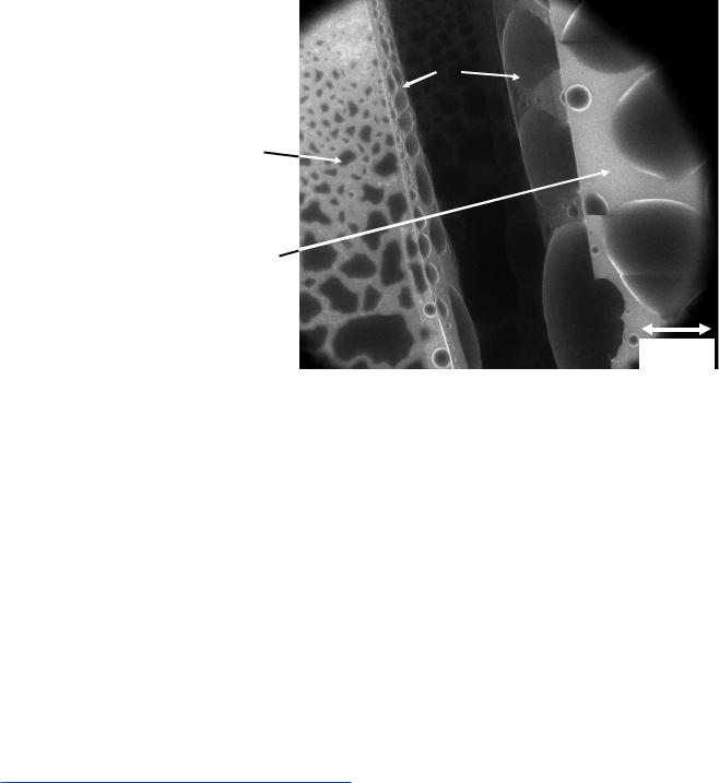
. Fig. 12.4 VPSEM imaging of water condensed in situ on silicon treated with a hydrophobic layer (octadecanethiol), a hydrophilic layer (erythrocyte membrane), and bare, uncoated silicon (nearly vertical fracture surfaces) (Example courtesy Scott Wight, NIST)
Hydrophilic monolayer on Si (erythrocyte membrane)
Hydrophobic monolayer on Si (octadecanethiol)
177 |
|
12 |
|
|
|
Bare Si
100 µm
with a cooling stage capable of reaching −5 °C to 5 °C. With careful control of both the pressure of water vapor added to the specimen chamber and of the specimen temperature, the microscopist can select the relative humidity in the sample chamber so that water can be evaporated, condensed, or maintained in liquid–gas or solid-gas equilibrium. In addition to direct examination of water-containing specimens, experiments can be performed in which the presence and quantity amount of water is controlled as a variable, enabling a wide range of chemical reactions to be observed. . Figure 12.4 shows an example of the condensation of water on a silicon wafer, one side of which was covered with a hydrophobic layer while the other was coated with a hydrophilic layer, directly revealing the differences in the wetting behavior on the two applied layers, as well as the bare silicon exposed by fracturing the specimen.
12.4\ Gas Scattering Modification
of the Focused Electron Beam
The differential pumping system achieves vacuum levels that minimize gas scattering and preserve the beam integrity as it passes from the electron source through the electron-optical column. As the beam emerges from the high vacuum of the electron column through the final aperture into the elevated pressure of the specimen chamber, the volume density of gas atoms rapidly increases, and with it the probability that elastic scattering events with the gas atoms will occur. Although the volume density of the gas atoms in the chamber is very low compared to the density of a solid material, the path length that the beam electrons must travel in the elevated pressure region of the sample chamber typically ranges from
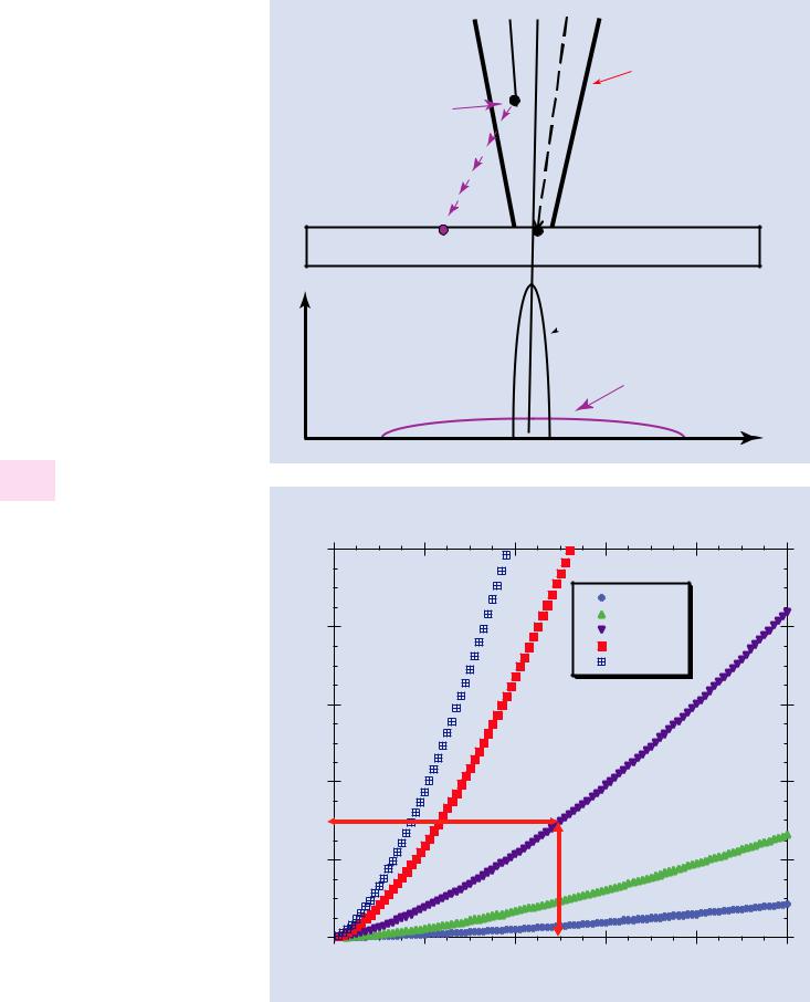
1 mm to 10 mm or more before reaching the specimen surface. As illustrated schematically in . Fig. 12.5, elastic scattering events that occur with the gas molecules along this path cause beam electrons to substantially deviate out of the focused beam to create a “skirt”. Even a small angle elastic event with a 1-degree scattering angle that occurs 1 mm above the specimen surface will cause the beam electron to be displaced by 17 μm radially from the focused beam.
How large is the gas-scattering skirt? The extent of the beam skirt can be estimated from the ideal gas law (the density of particles at a pressure p is given by n/V = p/RT, where n is the number of moles, V is the volume, R is the gas constant, and T is the temperature) and by using the cross section for elastic scattering for a single event (Danilatos 1988):
Rs = (0.364 Z / E)( p / T )1/ 2 L3/ 2 |
\ |
(12.1) |
|
|
where Rs = skirt radius (m) Z = atomic number of the gas E = beam energy (keV) p = pressure (Pa) T= temperature (K)
L = Gas Path Length (GPL) (m)
. Figure 12.6 plots the skirt radius for a beam energy of 20 keV as a function of the gas path length through oxygen at several different chamber pressures. For a pressure of 100 Pa and a gas path length of 5 mm, the skirt radius is calculated to be 30 μm. Consider the change in scale from the focused beam to the skirt that results from gas scattering. The high vacuum beam footprint that gives the lateral extent of the
BSE, SE, and X-ray production can be estimated with the
178\ Chapter 12 · Variable Pressure Scanning Electron Microscopy (VPSEM)
. Fig. 12.5 Schematic diagram showing gas scattering leading to development of the skirt surrounding the unscattered beam at the specimen surface
Intensity
Limit for 99 % of beam electrons
Elastic
scattering event with
gas atom
Unscattered
 beam intensity
Skirt intensity
|
|
|
|
|
|
|
Position |
12 |
|
|
|
|
|
|
|
. Fig. 12.6 Development of |
|
|
|
|
|
|
|
beam skirt for 20-keV electrons |
|
|
|
Development of Beam “Skirt” |
|
|
|
passing through oxygen at |
|
|
|
Gas Scattering Skirt (Oxygen; beam energy 20 keV) |
|
|
|
various pressures as calculated |
|
100 |
|
|
|
|
|
with Eq. 12.1 |
|
|
|
|
|
|
|
|
|
|
|
|
1 Pa |
|
|
|
|
80 |
|
|
10 Pa |
|
|
|
|
|
|
100 Pa |
|
|
|
|
|
|
|
|
1000 Pa |
|
|
|
(micrometers)Radius |
|
|
|
2500 Pa |
|
|
|
60 |
|
|
|
|
|
|
|
|
|
|
|
|
|
|
|
Skirt |
40 |
|
|
|
|
|
|
|
|
|
|
|
|
|
|
|
30 |
|
|
|
|
|
|
|
20 |
|
|
|
|
|
|
|
0 |
|
|
|
|
|
|
|
0 |
2 |
4 |
6 |
8 |
10 |
Gas Path Length (mm)
179 |
12 |
12.4 · Gas Scattering Modification of the Focused Electron Beam
Kanaya–Okayama range equation. For a copper specimen and E0 = 20 keV, the full range RK-O = 1.5 μm, which is also a good estimate of the diameter of the interaction volume projected on the entrance surface. With a beam/interaction volume footprint radius of 0.75 μm, the gas scattering skirt of 30-μm radius is thus a factor of 40 larger in linear dimension, and the skirt is a factor of 1600 larger in area than that due the focused beam and beam specimen interactions. Considering just a 10-nm incident beam diameter (5-nm radius), the gas scattering skirt is 6000 times larger.
While Eq. 12.1 is useful to estimate the extent of the gas scattering skirt under VPSEM conditions, it provides no information on the relative fraction of the beam that remains unscattered or on the distribution of gas-scattered electrons within the skirt. The Monte Carlo simulation embedded in NIST DTSA-II enables explicit treatment of gas scattering to provide detailed information on the unscattered beam electrons as well as the spatial distribution of electrons scattered
into the skirt. The VPSEM menu of DTSA-II allows selection of the critical variables: the gas path length, the gas pressure, and the gas species (He, N2, O2, H2O, or Ar). . Table 12.1 gives an example of the Monte Carlo output for the electron scattering out of the beam for a 5-mm gas path length through 100 Pa of water vapor. In addition to the radial distribution, the DTSA II Monte Carlo reports the unscattered fraction that remains in the focused beam, a value that is critical for estimating the likely success of VPSEM imaging, as described below.
. Figure 12.7a plots the gas scattering predicted by the Monte Carlo simulation for a gas path length of 5 mm and 100 Pa of O2, presented as the cumulative electron intensity as a function of radial distance out to 50 μm from the beam center. For these conditions the unscattered beam retains about 0.70 of the beam intensity that enters the specimen chamber. The skirt out to a radius of 30 μm contains a cumulative intensity of 0.84 of the incident beam
. Table 12.1 NIST DTSA-II Monte Carlo simulation for 20-keV electrons passing through 5 mm of water vapor at 100 Pa
Ring |
Inner Radius, |
Outer radius, |
Ring area, |
Electron count |
Electron |
Cumulative (%) |
|
μm |
μm |
μm2 |
|
fraction |
|
Undeflected |
— |
— |
— |
42,279 |
0.661 |
— |
|
|
|
|
|
|
|
1 |
0.0 |
2.5 |
19.6 |
46,789 |
0.731 |
73.1 |
2 |
2.5 |
5.0 |
58.9 |
2431 |
0.038 |
76.9 |
3 |
5.0 |
7.5 |
98.2 |
1457 |
0.023 |
79.2 |
4 |
7.5 |
10.0 |
137.4 |
1081 |
0.017 |
80.9 |
5 |
10.0 |
12.5 |
176.7 |
834 |
0.013 |
82.2 |
6 |
12.5 |
15.0 |
216.0 |
730 |
0.011 |
83.3 |
7 |
15.0 |
17.5 |
255.3 |
589 |
0.009 |
84.2 |
8 |
17.5 |
20.0 |
294.5 |
554 |
0.009 |
85.1 |
9 |
20.0 |
22.5 |
333.8 |
490 |
0.008 |
85.9 |
10 |
22.5 |
25.0 |
373.1 |
393 |
0.006 |
86.5 |
11 |
25.0 |
27.5 |
412.3 |
395 |
0.006 |
87.1 |
12 |
27.5 |
30.0 |
451.6 |
341 |
0.005 |
87.6 |
13 |
30.0 |
32.5 |
490.9 |
271 |
0.004 |
88.1 |
14 |
32.5 |
35.0 |
530.1 |
309 |
0.005 |
88.5 |
15 |
35.0 |
37.5 |
569.4 |
274 |
0.004 |
89.0 |
16 |
37.5 |
40.0 |
608.7 |
248 |
0.004 |
89.4 |
17 |
40.0 |
42.5 |
648.0 |
224 |
0.004 |
89.7 |
18 |
42.5 |
45.0 |
687.2 |
217 |
0.003 |
90.0 |
19 |
45.0 |
47.5 |
726.5 |
204 |
0.003 |
90.4 |
20 |
47.5 |
50.0 |
765.8 |
191 |
0.003 |
90.7 |
180\ Chapter 12 · Variable Pressure Scanning Electron Microscopy (VPSEM)
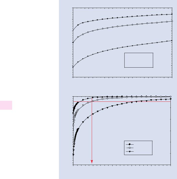
. Fig. 12.7 a Cumulative electron intensity as a function of distance (0–50 μm) from the beam center for 20-keV electrons passing through 100 Pa of oxygen as calculated with NIST DTSA-II. b Cumulative electron intensity as a function of distance (0–1000 μm) from the beam center for 20-keV electrons passing through 100 Pa of oxygen as calculated with NIST DTSA-II (GPL = Gas Path Length)
12
a
Cumulative electron intensity
b
Cumulative electron intensity
1.0
0.9
0.8 
0.7 
0.6
0.5
0.4
0
1.0
0.9
0.8 
0.7 
0.6
0.5
0.4
0
VPSEM 100 Pa O2
 3 mm GPL
 5 mm GPL
  10 mm GPL
10 |
20 |
30 |
40 |
50 |
Radial distance from beam center (micrometers)
VPSEM 100 Pa O2
3 mm GPL
5 mm GPL
10 mm GPL
200 |
400 |
600 |
800 |
1000 |
Radial distance from beam center (micrometers)
current. To capture 0.95 of the total beam current requires a radial distance to approximately 190 μm, as shown in
. Fig. 12.7b, and the last 0.05 of the beam electrons are distributed out to 1000 μm (1 mm). The strong effect of the
gas path length on the skirt radius, which follows a 3/2 exponent in the scattering Eq. 12.1, can be seen in
. Fig. 12.7 by comparing the plots for 3-, 5-, and 10-mm gas path lengths.