

- •Preface
- •Imaging Microscopic Features
- •Measuring the Crystal Structure
- •References
- •Contents
- •1.4 Simulating the Effects of Elastic Scattering: Monte Carlo Calculations
- •What Are the Main Features of the Beam Electron Interaction Volume?
- •How Does the Interaction Volume Change with Composition?
- •How Does the Interaction Volume Change with Incident Beam Energy?
- •How Does the Interaction Volume Change with Specimen Tilt?
- •1.5 A Range Equation To Estimate the Size of the Interaction Volume
- •References
- •2: Backscattered Electrons
- •2.1 Origin
- •2.2.1 BSE Response to Specimen Composition (η vs. Atomic Number, Z)
- •SEM Image Contrast with BSE: “Atomic Number Contrast”
- •SEM Image Contrast: “BSE Topographic Contrast—Number Effects”
- •2.2.3 Angular Distribution of Backscattering
- •Beam Incident at an Acute Angle to the Specimen Surface (Specimen Tilt > 0°)
- •SEM Image Contrast: “BSE Topographic Contrast—Trajectory Effects”
- •2.2.4 Spatial Distribution of Backscattering
- •Depth Distribution of Backscattering
- •Radial Distribution of Backscattered Electrons
- •2.3 Summary
- •References
- •3: Secondary Electrons
- •3.1 Origin
- •3.2 Energy Distribution
- •3.3 Escape Depth of Secondary Electrons
- •3.8 Spatial Characteristics of Secondary Electrons
- •References
- •4: X-Rays
- •4.1 Overview
- •4.2 Characteristic X-Rays
- •4.2.1 Origin
- •4.2.2 Fluorescence Yield
- •4.2.3 X-Ray Families
- •4.2.4 X-Ray Nomenclature
- •4.2.6 Characteristic X-Ray Intensity
- •Isolated Atoms
- •X-Ray Production in Thin Foils
- •X-Ray Intensity Emitted from Thick, Solid Specimens
- •4.3 X-Ray Continuum (bremsstrahlung)
- •4.3.1 X-Ray Continuum Intensity
- •4.3.3 Range of X-ray Production
- •4.4 X-Ray Absorption
- •4.5 X-Ray Fluorescence
- •References
- •5.1 Electron Beam Parameters
- •5.2 Electron Optical Parameters
- •5.2.1 Beam Energy
- •Landing Energy
- •5.2.2 Beam Diameter
- •5.2.3 Beam Current
- •5.2.4 Beam Current Density
- •5.2.5 Beam Convergence Angle, α
- •5.2.6 Beam Solid Angle
- •5.2.7 Electron Optical Brightness, β
- •Brightness Equation
- •5.2.8 Focus
- •Astigmatism
- •5.3 SEM Imaging Modes
- •5.3.1 High Depth-of-Field Mode
- •5.3.2 High-Current Mode
- •5.3.3 Resolution Mode
- •5.3.4 Low-Voltage Mode
- •5.4 Electron Detectors
- •5.4.1 Important Properties of BSE and SE for Detector Design and Operation
- •Abundance
- •Angular Distribution
- •Kinetic Energy Response
- •5.4.2 Detector Characteristics
- •Angular Measures for Electron Detectors
- •Elevation (Take-Off) Angle, ψ, and Azimuthal Angle, ζ
- •Solid Angle, Ω
- •Energy Response
- •Bandwidth
- •5.4.3 Common Types of Electron Detectors
- •Backscattered Electrons
- •Passive Detectors
- •Scintillation Detectors
- •Semiconductor BSE Detectors
- •5.4.4 Secondary Electron Detectors
- •Everhart–Thornley Detector
- •Through-the-Lens (TTL) Electron Detectors
- •TTL SE Detector
- •TTL BSE Detector
- •Measuring the DQE: BSE Semiconductor Detector
- •References
- •6: Image Formation
- •6.1 Image Construction by Scanning Action
- •6.2 Magnification
- •6.3 Making Dimensional Measurements With the SEM: How Big Is That Feature?
- •Using a Calibrated Structure in ImageJ-Fiji
- •6.4 Image Defects
- •6.4.1 Projection Distortion (Foreshortening)
- •6.4.2 Image Defocusing (Blurring)
- •6.5 Making Measurements on Surfaces With Arbitrary Topography: Stereomicroscopy
- •6.5.1 Qualitative Stereomicroscopy
- •Fixed beam, Specimen Position Altered
- •Fixed Specimen, Beam Incidence Angle Changed
- •6.5.2 Quantitative Stereomicroscopy
- •Measuring a Simple Vertical Displacement
- •References
- •7: SEM Image Interpretation
- •7.1 Information in SEM Images
- •7.2.2 Calculating Atomic Number Contrast
- •Establishing a Robust Light-Optical Analogy
- •Getting It Wrong: Breaking the Light-Optical Analogy of the Everhart–Thornley (Positive Bias) Detector
- •Deconstructing the SEM/E–T Image of Topography
- •SUM Mode (A + B)
- •DIFFERENCE Mode (A−B)
- •References
- •References
- •9: Image Defects
- •9.1 Charging
- •9.1.1 What Is Specimen Charging?
- •9.1.3 Techniques to Control Charging Artifacts (High Vacuum Instruments)
- •Observing Uncoated Specimens
- •Coating an Insulating Specimen for Charge Dissipation
- •Choosing the Coating for Imaging Morphology
- •9.2 Radiation Damage
- •9.3 Contamination
- •References
- •10: High Resolution Imaging
- •10.2 Instrumentation Considerations
- •10.4.1 SE Range Effects Produce Bright Edges (Isolated Edges)
- •10.4.4 Too Much of a Good Thing: The Bright Edge Effect Hinders Locating the True Position of an Edge for Critical Dimension Metrology
- •10.5.1 Beam Energy Strategies
- •Low Beam Energy Strategy
- •High Beam Energy Strategy
- •Making More SE1: Apply a Thin High-δ Metal Coating
- •Making Fewer BSEs, SE2, and SE3 by Eliminating Bulk Scattering From the Substrate
- •10.6 Factors That Hinder Achieving High Resolution
- •10.6.2 Pathological Specimen Behavior
- •Contamination
- •Instabilities
- •References
- •11: Low Beam Energy SEM
- •11.3 Selecting the Beam Energy to Control the Spatial Sampling of Imaging Signals
- •11.3.1 Low Beam Energy for High Lateral Resolution SEM
- •11.3.2 Low Beam Energy for High Depth Resolution SEM
- •11.3.3 Extremely Low Beam Energy Imaging
- •References
- •12.1.1 Stable Electron Source Operation
- •12.1.2 Maintaining Beam Integrity
- •12.1.4 Minimizing Contamination
- •12.3.1 Control of Specimen Charging
- •12.5 VPSEM Image Resolution
- •References
- •13: ImageJ and Fiji
- •13.1 The ImageJ Universe
- •13.2 Fiji
- •13.3 Plugins
- •13.4 Where to Learn More
- •References
- •14: SEM Imaging Checklist
- •14.1.1 Conducting or Semiconducting Specimens
- •14.1.2 Insulating Specimens
- •14.2 Electron Signals Available
- •14.2.1 Beam Electron Range
- •14.2.2 Backscattered Electrons
- •14.2.3 Secondary Electrons
- •14.3 Selecting the Electron Detector
- •14.3.2 Backscattered Electron Detectors
- •14.3.3 “Through-the-Lens” Detectors
- •14.4 Selecting the Beam Energy for SEM Imaging
- •14.4.4 High Resolution SEM Imaging
- •Strategy 1
- •Strategy 2
- •14.5 Selecting the Beam Current
- •14.5.1 High Resolution Imaging
- •14.5.2 Low Contrast Features Require High Beam Current and/or Long Frame Time to Establish Visibility
- •14.6 Image Presentation
- •14.6.1 “Live” Display Adjustments
- •14.6.2 Post-Collection Processing
- •14.7 Image Interpretation
- •14.7.1 Observer’s Point of View
- •14.7.3 Contrast Encoding
- •14.8.1 VPSEM Advantages
- •14.8.2 VPSEM Disadvantages
- •15: SEM Case Studies
- •15.1 Case Study: How High Is That Feature Relative to Another?
- •15.2 Revealing Shallow Surface Relief
- •16.1.2 Minor Artifacts: The Si-Escape Peak
- •16.1.3 Minor Artifacts: Coincidence Peaks
- •16.1.4 Minor Artifacts: Si Absorption Edge and Si Internal Fluorescence Peak
- •16.2 “Best Practices” for Electron-Excited EDS Operation
- •16.2.1 Operation of the EDS System
- •Choosing the EDS Time Constant (Resolution and Throughput)
- •Choosing the Solid Angle of the EDS
- •Selecting a Beam Current for an Acceptable Level of System Dead-Time
- •16.3.1 Detector Geometry
- •16.3.2 Process Time
- •16.3.3 Optimal Working Distance
- •16.3.4 Detector Orientation
- •16.3.5 Count Rate Linearity
- •16.3.6 Energy Calibration Linearity
- •16.3.7 Other Items
- •16.3.8 Setting Up a Quality Control Program
- •Using the QC Tools Within DTSA-II
- •Creating a QC Project
- •Linearity of Output Count Rate with Live-Time Dose
- •Resolution and Peak Position Stability with Count Rate
- •Solid Angle for Low X-ray Flux
- •Maximizing Throughput at Moderate Resolution
- •References
- •17: DTSA-II EDS Software
- •17.1 Getting Started With NIST DTSA-II
- •17.1.1 Motivation
- •17.1.2 Platform
- •17.1.3 Overview
- •17.1.4 Design
- •Simulation
- •Quantification
- •Experiment Design
- •Modeled Detectors (. Fig. 17.1)
- •Window Type (. Fig. 17.2)
- •The Optimal Working Distance (. Figs. 17.3 and 17.4)
- •Elevation Angle
- •Sample-to-Detector Distance
- •Detector Area
- •Crystal Thickness
- •Number of Channels, Energy Scale, and Zero Offset
- •Resolution at Mn Kα (Approximate)
- •Azimuthal Angle
- •Gold Layer, Aluminum Layer, Nickel Layer
- •Dead Layer
- •Zero Strobe Discriminator (. Figs. 17.7 and 17.8)
- •Material Editor Dialog (. Figs. 17.9, 17.10, 17.11, 17.12, 17.13, and 17.14)
- •17.2.1 Introduction
- •17.2.2 Monte Carlo Simulation
- •17.2.4 Optional Tables
- •References
- •18: Qualitative Elemental Analysis by Energy Dispersive X-Ray Spectrometry
- •18.1 Quality Assurance Issues for Qualitative Analysis: EDS Calibration
- •18.2 Principles of Qualitative EDS Analysis
- •Exciting Characteristic X-Rays
- •Fluorescence Yield
- •X-ray Absorption
- •Si Escape Peak
- •Coincidence Peaks
- •18.3 Performing Manual Qualitative Analysis
- •Beam Energy
- •Choosing the EDS Resolution (Detector Time Constant)
- •Obtaining Adequate Counts
- •18.4.1 Employ the Available Software Tools
- •18.4.3 Lower Photon Energy Region
- •18.4.5 Checking Your Work
- •18.5 A Worked Example of Manual Peak Identification
- •References
- •19.1 What Is a k-ratio?
- •19.3 Sets of k-ratios
- •19.5 The Analytical Total
- •19.6 Normalization
- •19.7.1 Oxygen by Assumed Stoichiometry
- •19.7.3 Element by Difference
- •19.8 Ways of Reporting Composition
- •19.8.1 Mass Fraction
- •19.8.2 Atomic Fraction
- •19.8.3 Stoichiometry
- •19.8.4 Oxide Fractions
- •Example Calculations
- •19.9 The Accuracy of Quantitative Electron-Excited X-ray Microanalysis
- •19.9.1 Standards-Based k-ratio Protocol
- •19.9.2 “Standardless Analysis”
- •19.10 Appendix
- •19.10.1 The Need for Matrix Corrections To Achieve Quantitative Analysis
- •19.10.2 The Physical Origin of Matrix Effects
- •19.10.3 ZAF Factors in Microanalysis
- •X-ray Generation With Depth, φ(ρz)
- •X-ray Absorption Effect, A
- •X-ray Fluorescence, F
- •References
- •20.2 Instrumentation Requirements
- •20.2.1 Choosing the EDS Parameters
- •EDS Spectrum Channel Energy Width and Spectrum Energy Span
- •EDS Time Constant (Resolution and Throughput)
- •EDS Calibration
- •EDS Solid Angle
- •20.2.2 Choosing the Beam Energy, E0
- •20.2.3 Measuring the Beam Current
- •20.2.4 Choosing the Beam Current
- •Optimizing Analysis Strategy
- •20.3.4 Ba-Ti Interference in BaTiSi3O9
- •20.4 The Need for an Iterative Qualitative and Quantitative Analysis Strategy
- •20.4.2 Analysis of a Stainless Steel
- •20.5 Is the Specimen Homogeneous?
- •20.6 Beam-Sensitive Specimens
- •20.6.1 Alkali Element Migration
- •20.6.2 Materials Subject to Mass Loss During Electron Bombardment—the Marshall-Hall Method
- •Thin Section Analysis
- •Bulk Biological and Organic Specimens
- •References
- •21: Trace Analysis by SEM/EDS
- •21.1 Limits of Detection for SEM/EDS Microanalysis
- •21.2.1 Estimating CDL from a Trace or Minor Constituent from Measuring a Known Standard
- •21.2.2 Estimating CDL After Determination of a Minor or Trace Constituent with Severe Peak Interference from a Major Constituent
- •21.3 Measurements of Trace Constituents by Electron-Excited Energy Dispersive X-ray Spectrometry
- •The Inevitable Physics of Remote Excitation Within the Specimen: Secondary Fluorescence Beyond the Electron Interaction Volume
- •Simulation of Long-Range Secondary X-ray Fluorescence
- •NIST DTSA II Simulation: Vertical Interface Between Two Regions of Different Composition in a Flat Bulk Target
- •NIST DTSA II Simulation: Cubic Particle Embedded in a Bulk Matrix
- •21.5 Summary
- •References
- •22.1.2 Low Beam Energy Analysis Range
- •22.2 Advantage of Low Beam Energy X-Ray Microanalysis
- •22.2.1 Improved Spatial Resolution
- •22.3 Challenges and Limitations of Low Beam Energy X-Ray Microanalysis
- •22.3.1 Reduced Access to Elements
- •22.3.3 At Low Beam Energy, Almost Everything Is Found To Be Layered
- •Analysis of Surface Contamination
- •References
- •23: Analysis of Specimens with Special Geometry: Irregular Bulk Objects and Particles
- •23.2.1 No Chemical Etching
- •23.3 Consequences of Attempting Analysis of Bulk Materials With Rough Surfaces
- •23.4.1 The Raw Analytical Total
- •23.4.2 The Shape of the EDS Spectrum
- •23.5 Best Practices for Analysis of Rough Bulk Samples
- •23.6 Particle Analysis
- •Particle Sample Preparation: Bulk Substrate
- •The Importance of Beam Placement
- •Overscanning
- •“Particle Mass Effect”
- •“Particle Absorption Effect”
- •The Analytical Total Reveals the Impact of Particle Effects
- •Does Overscanning Help?
- •23.6.6 Peak-to-Background (P/B) Method
- •Specimen Geometry Severely Affects the k-ratio, but Not the P/B
- •Using the P/B Correspondence
- •23.7 Summary
- •References
- •24: Compositional Mapping
- •24.2 X-Ray Spectrum Imaging
- •24.2.1 Utilizing XSI Datacubes
- •24.2.2 Derived Spectra
- •SUM Spectrum
- •MAXIMUM PIXEL Spectrum
- •24.3 Quantitative Compositional Mapping
- •24.4 Strategy for XSI Elemental Mapping Data Collection
- •24.4.1 Choosing the EDS Dead-Time
- •24.4.2 Choosing the Pixel Density
- •24.4.3 Choosing the Pixel Dwell Time
- •“Flash Mapping”
- •High Count Mapping
- •References
- •25.1 Gas Scattering Effects in the VPSEM
- •25.1.1 Why Doesn’t the EDS Collimator Exclude the Remote Skirt X-Rays?
- •25.2 What Can Be Done To Minimize gas Scattering in VPSEM?
- •25.2.2 Favorable Sample Characteristics
- •Particle Analysis
- •25.2.3 Unfavorable Sample Characteristics
- •References
- •26.1 Instrumentation
- •26.1.2 EDS Detector
- •26.1.3 Probe Current Measurement Device
- •Direct Measurement: Using a Faraday Cup and Picoammeter
- •A Faraday Cup
- •Electrically Isolated Stage
- •Indirect Measurement: Using a Calibration Spectrum
- •26.1.4 Conductive Coating
- •26.2 Sample Preparation
- •26.2.1 Standard Materials
- •26.2.2 Peak Reference Materials
- •26.3 Initial Set-Up
- •26.3.1 Calibrating the EDS Detector
- •Selecting a Pulse Process Time Constant
- •Energy Calibration
- •Quality Control
- •Sample Orientation
- •Detector Position
- •Probe Current
- •26.4 Collecting Data
- •26.4.1 Exploratory Spectrum
- •26.4.2 Experiment Optimization
- •26.4.3 Selecting Standards
- •26.4.4 Reference Spectra
- •26.4.5 Collecting Standards
- •26.4.6 Collecting Peak-Fitting References
- •26.5 Data Analysis
- •26.5.2 Quantification
- •26.6 Quality Check
- •Reference
- •27.2 Case Study: Aluminum Wire Failures in Residential Wiring
- •References
- •28: Cathodoluminescence
- •28.1 Origin
- •28.2 Measuring Cathodoluminescence
- •28.3 Applications of CL
- •28.3.1 Geology
- •Carbonado Diamond
- •Ancient Impact Zircons
- •28.3.2 Materials Science
- •Semiconductors
- •Lead-Acid Battery Plate Reactions
- •28.3.3 Organic Compounds
- •References
- •29.1.1 Single Crystals
- •29.1.2 Polycrystalline Materials
- •29.1.3 Conditions for Detecting Electron Channeling Contrast
- •Specimen Preparation
- •Instrument Conditions
- •29.2.1 Origin of EBSD Patterns
- •29.2.2 Cameras for EBSD Pattern Detection
- •29.2.3 EBSD Spatial Resolution
- •29.2.5 Steps in Typical EBSD Measurements
- •Sample Preparation for EBSD
- •Align Sample in the SEM
- •Check for EBSD Patterns
- •Adjust SEM and Select EBSD Map Parameters
- •Run the Automated Map
- •29.2.6 Display of the Acquired Data
- •29.2.7 Other Map Components
- •29.2.10 Application Example
- •Application of EBSD To Understand Meteorite Formation
- •29.2.11 Summary
- •Specimen Considerations
- •EBSD Detector
- •Selection of Candidate Crystallographic Phases
- •Microscope Operating Conditions and Pattern Optimization
- •Selection of EBSD Acquisition Parameters
- •Collect the Orientation Map
- •References
- •30.1 Introduction
- •30.2 Ion–Solid Interactions
- •30.3 Focused Ion Beam Systems
- •30.5 Preparation of Samples for SEM
- •30.5.1 Cross-Section Preparation
- •30.5.2 FIB Sample Preparation for 3D Techniques and Imaging
- •30.6 Summary
- •References
- •31: Ion Beam Microscopy
- •31.1 What Is So Useful About Ions?
- •31.2 Generating Ion Beams
- •31.3 Signal Generation in the HIM
- •31.5 Patterning with Ion Beams
- •31.7 Chemical Microanalysis with Ion Beams
- •References
- •Appendix
- •A Database of Electron–Solid Interactions
- •A Database of Electron–Solid Interactions
- •Introduction
- •Backscattered Electrons
- •Secondary Yields
- •Stopping Powers
- •X-ray Ionization Cross Sections
- •Conclusions
- •References
- •Index
- •Reference List
- •Index
\424 Chapter 24 · Compositional Mapping
Log10 Counts
Counts
Al
1000000 |
NiL |
|
|
|
|
|
|
|
|
|
|
FINAL_-1900u-Mask_ |
|
|
|
|
|
|
|
|
|
|
|
||||
|
|
|
|
|
|
|
|
|
|
|
highFe_phase |
|
|
|
|
NiL |
+ Al |
|
|
|
|
|
Ni |
|
|
|
|
100000 |
|
|
|
|
|
Fe |
|
|
|
|
|
||
|
Al + |
Al |
|
|
|
|
|
|
|
|
|
||
|
|
|
|
|
|
|
|
|
|
|
|||
|
|
|
|
|
|
|
|
|
|
|
|
||
10000 |
|
|
|
|
|
|
|
|
|
|
|
|
|
|
|
|
|
|
|
|
|
|
|
|
|
|
|
1000 |
|
|
|
|
|
Al Fe Ni |
|
|
|
|
|
|
|
|
|
|
|
|
|
|
|
|
|
|
|
|
|
100 |
|
|
|
|
|
|
|
|
|
|
|
|
|
0 |
1 |
2 |
3 |
4 |
|
6 |
7 |
8 |
9 |
10 |
|||
50000 |
|
|
|
20 µm |
|
|
|
|
|
|
|
FINAL_-1900u-Mask_ |
|
|
|
|
|
|
|
|
|
|
|
|
|
||
|
|
|
|
|
|
|
|
|
|
|
|
||
|
|
|
|
|
|
|
|
|
|
|
|
||
45000 |
|
|
|
|
|
|
|
|
|
|
|
highFe_phase |
|
|
|
+ Al |
|
|
|
|
|
|
|
|
|
|
|
40000 |
|
|
|
|
|
|
|
|
|
|
|
|
|
35000 |
|
|
Al |
|
|
|
|
|
|
|
|
|
|
|
NiL |
|
|
|
|
|
|
|
|
|
|
|
|
30000 |
|
|
|
|
|
|
|
|
|
|
|
|
|
25000 |
|
+ |
|
Fe mask |
|
|
|
|
|
|
|
|
|
|
Al |
|
|
|
|
|
|
|
|
|
|
||
|
|
|
|
|
|
|
|
|
|
|
|
|
|
20000 |
|
|
|
|
|
|
|
|
|
|
|
|
|
15000 |
|
|
|
|
|
|
|
|
|
|
|
|
|
10000 |
|
|
|
|
|
|
|
|
|
|
|
|
|
5000 |
|
|
|
|
|
|
|
|
|
|
|
|
|
0 |
|
|
|
|
|
|
|
|
|
|
|
|
|
0 |
1 |
2 |
3 |
4 |
5 |
6 |
7 |
8 |
9 |
10 |
|||
Photon Energy (keV)
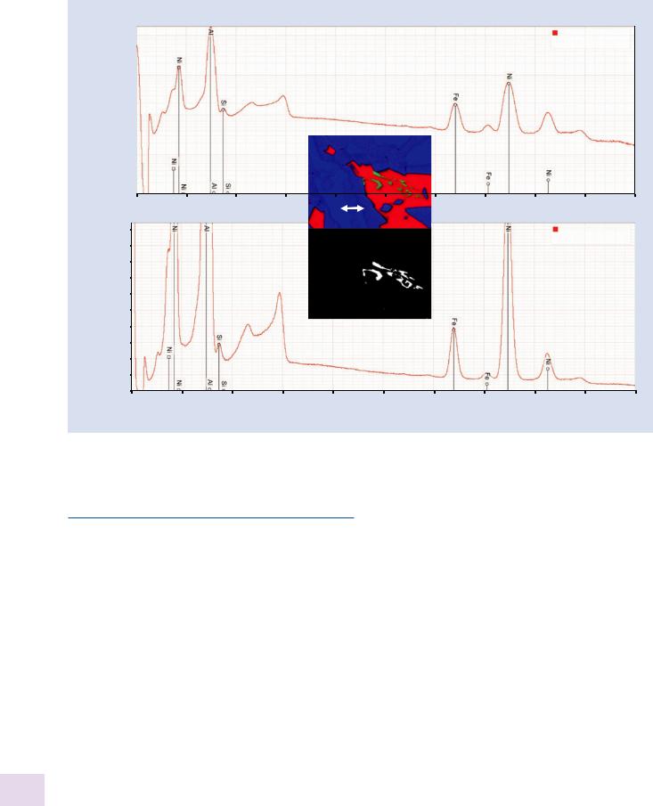
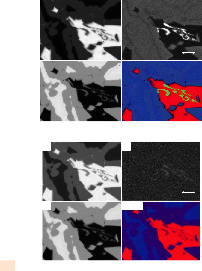
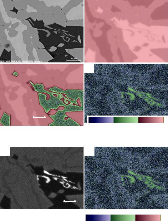
. Fig. 24.10 Creation of a pixel mask (inset) using the Fe elemental map for Raney nickel to select pixels from which a SUM spectrum is constructed for the Fe-rich phase
24.3\ Quantitative Compositional Mapping
The XSI contains the complete EDS spectrum at each pixel (or the position-tagged photon database that can be used to reconstruct the individual pixel spectra). Quantitative compositional mapping implements the normal fixed measurement location quantitative analysis procedure at every pixel in a map. Qualitative analysis is first performed to identify the peaks in the SUM and MAXIMUM PIXEL spectra of the XSI to determine the suite of elements present within the mapped area, noting that all elements are unlikely to be present at every pixel. The pixel-level EDS spectra can then be individually processed following the same quantitative analysis protocol used for individually measured spectra, ultimately replacing the gray or color scale in total intensity elemental maps, which are based on raw X-ray intensities and which are nearly impossible to compare, with a gray or color scale based on the calculated concentrations, which can be sensibly compared. Most vendor compositional mapping software extracts characteristic peak intensities by applying multiple linear
24 least squares (MLLS) peak fitting or alternatively fits a background model under the peaks. These extracted pixel-level
elemental intensities are then quantified by a “standardless analysis” procedure to calculate the individual pixel concentration values. Alternatively, rigorous standards-based quantitative analysis can be performed on the pixel-level intensity data with NIST DTSA II by utilizing the scripting language to sequentially calculate the pixel spectra in a datacube. MLLS peak fitting to extract the characteristic intensities, k-ratio calculation relative to a library of measured standards, and matrix corrections to yield the local concentrations of these elements for each pixel. An example of the NIST DTSA-II procedure applied to an XSI measured on the manganese nodule example of . Fig. 24.2 is presented in . Fig. 24.11, where the Fe K-L2,3 total intensity map, which suffers significant interference from Mn K-M2,3, shows a change in the apparent level of Fe in the center of the image after quantitative correction, as well as changes in several finer-scale details.
Quantitative compositional maps for major constituents displayed as gray-scale images are virtually identical to raw intensity elemental maps, as shown for the major constituents Al and Ni in . Figs. 24.12 and 24.13. Significant differences between raw intensity maps and compositional maps are found for minor and trace constituents, where correction
24.3 · Quantitative Compositional Mapping
. Fig. 24.11 Quantitative compositional mapping with DTSA-II on the XSI of a deepsea manganese nodule from
. Fig. 24.2: direct comparison of the total intensity map for Fe and the quantitative compositional map of Fe; note the decrease in the apparent Fe in the high Mn portion in the center of the image after quantification and local changes indicated by arrows (yellow shows extension of high Fe region; magenta shows elimination of dark features)
425 |
|
24 |
|
|
|
 Raw Fe K-L2,3 + Mn K-M2,3
Fe K-L2,3 after DTSA-II quantification
20 µm 
for the continuum background significantly changes the gray-scale image. As shown for the minor Fe constituent in
. Figs. 24.12 and 24.13, the false Fe contrast between the Nirich and Al-rich phases that arises due to the atomic number dependence of the X-ray continuum is eliminated in the Fe compositional map.
While rendering the underlying pixel data of quantitative compositional maps in gray scale is a useful starting point, the problem of achieving a quantitatively meaningful display remains. Because of autoscaling, the gray scales of the Al, Ni, and Fe maps in . Fig. 24.12 do not have the same numerical meaning. The Al and Ni concentrations locally reach high enough levels to correspond to brighter gray levels and have sufficient range to create strong contrast with direct gray-scale encoding, as seen in . Figs. 24.12 and 24.13. The Fe constituent which is present at a concentration with a maximum of approximately 0.04 mass fraction (4 wt %) never exceeds the minor constituent range, so the Fe map appears dark with little contrast in the quantitative map of . Fig. 24.13. Autoscaling of the Fe-map in
. Fig. 24.14 improves the contrast, but the same limitations
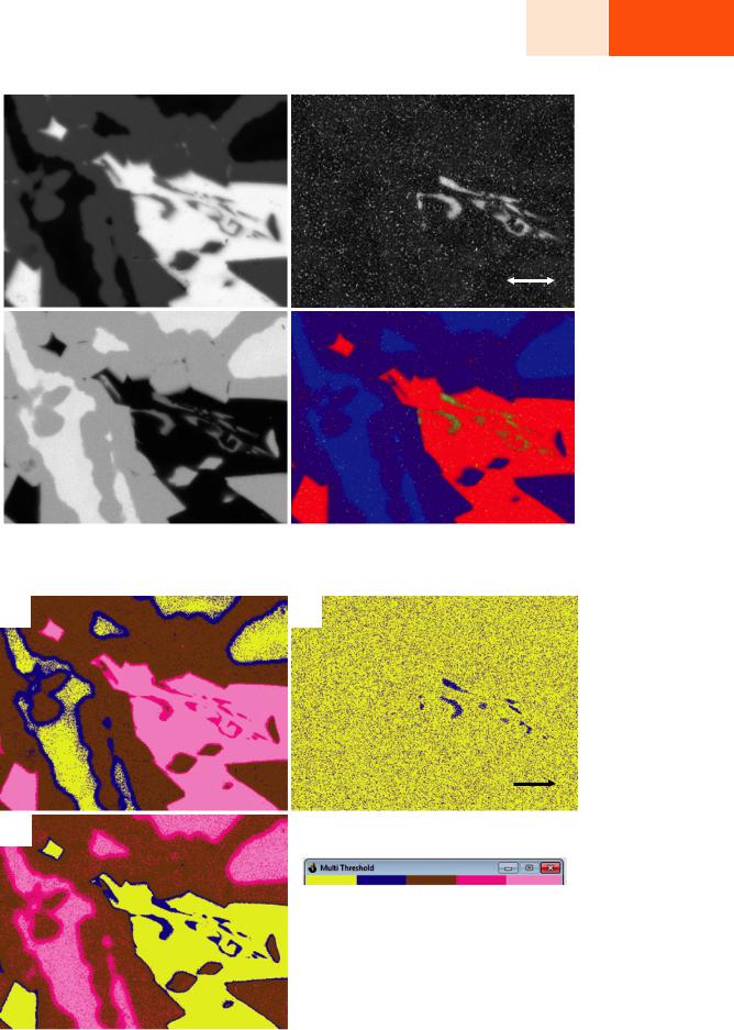
of autoscaling noted above still apply. Various pseudo-color scales, in which bands of contrasting colors are applied to the underlying data, are typically available in image processing software. Such pseudo-color scale can partially overcome the display limitations of gray-scale presentation, but the resulting images are often difficult to interpret. An example of a five band pseudo-color scale applied to the compositional maps using NIST Lispix is shown in
. Fig. 24.15. An effective display scheme for quantitative elemental maps that enables a viewer to readily compare concentrations of different elements spanning major, minor and trace ranges can be achieved with the Logarithmic Three-Band Encoding (Newbury and Bright 1999). A band of colors is assigned to each decade of the concentration range with the following characteristics:
Major: C > 0.1 to 1 (mass fraction) deep red to red pastel
Minor: 0.01 ≤C ≤0.1 deep green to green pastel Trace: 0.001 ≤C < 0.01 deep blue to blue pastel
The quantitative elemental maps are displayed with Logarithmic Three-Band Encoding in . Fig. 24.16, and the
\426 Chapter 24 · Compositional Mapping
Al |
|
Fe |
|
|
|
20 µm
Ni |
|
Al Fe Ni |
|
|
|
. Fig. 24.12 Raney nickel alloy XSI: total intensity maps for Al, Fe, and Ni with color overlay
Al |
Fe |
20 µm
Ni |
Al Fe Ni |
24 |
. Fig. 24.13 Quantitative compositional maps of the Raney nickel alloy XSI in 24.13; note low contrast in the Fe image presented without |
autoscaling
427 |
24 |
24.3 · Quantitative Compositional Mapping
Al |
|
Fe |
|
|
|
20 µm
Ni |
|
Al Fe Ni |
|
|
|
. Fig. 24.14 Quantitative compositional maps Raney nickel alloy XSI with contrast enhancement of the Fe map
Al |
Fe |
 20 µm
20 µm
Ni
0 |
50 |
100 |
150 |
200 |
255 |
. Fig. 24.15 Five band pseudo-color presentation of the quantitative compositional maps for Al, Fe, and Ni derived from the Raney nickel alloy XSI
\428 Chapter 24 · Compositional Mapping
major-minor-trace spatial relationships among the elemental constituents are readily discernible.
The Logarithmic Three-Band Encoding of the Fe compositional map in . Fig. 24.16 reveals apparent Fe contrast in the Al-rich and Fe-rich phases, and this contrast differs markedly
from the atomic-number dependence of the X-ray continuum seen in the raw Fe intensity image, as shown in . Fig. 24.17. The Logarithmic Three-Band Encoding shows that this apparent contrast occurs near the lower limit of the trace range. Is this trace Fe contrast meaningful or merely an uncorrected
BSE |
|
Al |
|
|
|
Ni |
Fe |
|
|
20 µm
0.001 |
0.01 |
0.1 |
1.0 |
0.1 |
1.0 |
10 |
100 wt% |
. Fig. 24.16 Logarithmic Three-Band Color encoding of the quantitative compositional maps for Al, Fe, and Ni derived from the Raney nickel alloy XSI
Fe |
Fe |
20 µm
Fe raw intensity elemental map
0.001 |
0.01 |
0.1 |
1.0 |
0.1 |
1.0 |
10 |
100 wt% |
Fe compositional map
24 |
. Fig. 24.17 Direct comparison of the Fe total intensity map and the Logarithmic Three-Band Encoding of the Fe quantitative compositional |
|
map. Note the distinct changes in the contrast within the trace concentration (C < 0.01) regions of the image |
|
24.3 · Quantitative Compositional Mapping
1000000
(Log) |
100000 |
|
|
Counts |
10000 |
|
|
|
1000 |
|
100 |
0
|
24000 |
|
|
22000 |
|
|
20000 |
|
|
18000 |
|
Counts |
16000 |
|
14000 |
||
|
12000
10000
8000
6000
4000
2000
0 
0
1 2
1 2
429 |
|
24 |
||
|
|
|
|
|
|
|
|
|
|
|
|
|
|
|
3 |
4 |
5 |
6 |
7 |
8 |
9 |
10 |
|
|
|
Energy (keV) |
|
|
|
|
|
|
|
|
|
|
|
|
|
|
|
|
|
|
|
|
|
|
|
|
3 |
4 |
5 |
6 |
7 |
8 |
9 |
10 |
|
|
Energy (keV) |
|
|
|
|
|
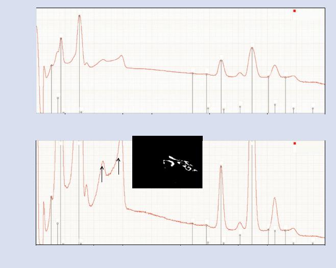
. Fig. 24.18 Raney nickel alloy XSI: mask of pixels corresponding to the Fe-rich phase and the corresponding SUM spectrum; the Fe peak corresponds to C=0.044 mass fraction
artifact? To examine this question, the analyst can use pixel masks of each phase selected from the Ni compositional map (or the BSE image) to obtain the SUM spectrum, as shown in
. Figs. 24.18 (Fe-rich phase), 24.19 (Al-rich phase), 24.20 (Ni-intermediate phase), and 24.21 (Ni-rich phase). These SUM spectra confirm that Fe is indeed present as a trace
constituent, with its highest level in the intermediate-Ni phase where CFe = 0.0027 (2700 ppm), falling to CFe = 0.00038 (380 ppm) in the high-Ni phase and to CFe = 0.00030 (300 ppm) in the high-Al phase. Additionally, trace Cr at a similar concentration is found in the Al-rich phase along with the trace Fe.