

- •Preface
- •Imaging Microscopic Features
- •Measuring the Crystal Structure
- •References
- •Contents
- •1.4 Simulating the Effects of Elastic Scattering: Monte Carlo Calculations
- •What Are the Main Features of the Beam Electron Interaction Volume?
- •How Does the Interaction Volume Change with Composition?
- •How Does the Interaction Volume Change with Incident Beam Energy?
- •How Does the Interaction Volume Change with Specimen Tilt?
- •1.5 A Range Equation To Estimate the Size of the Interaction Volume
- •References
- •2: Backscattered Electrons
- •2.1 Origin
- •2.2.1 BSE Response to Specimen Composition (η vs. Atomic Number, Z)
- •SEM Image Contrast with BSE: “Atomic Number Contrast”
- •SEM Image Contrast: “BSE Topographic Contrast—Number Effects”
- •2.2.3 Angular Distribution of Backscattering
- •Beam Incident at an Acute Angle to the Specimen Surface (Specimen Tilt > 0°)
- •SEM Image Contrast: “BSE Topographic Contrast—Trajectory Effects”
- •2.2.4 Spatial Distribution of Backscattering
- •Depth Distribution of Backscattering
- •Radial Distribution of Backscattered Electrons
- •2.3 Summary
- •References
- •3: Secondary Electrons
- •3.1 Origin
- •3.2 Energy Distribution
- •3.3 Escape Depth of Secondary Electrons
- •3.8 Spatial Characteristics of Secondary Electrons
- •References
- •4: X-Rays
- •4.1 Overview
- •4.2 Characteristic X-Rays
- •4.2.1 Origin
- •4.2.2 Fluorescence Yield
- •4.2.3 X-Ray Families
- •4.2.4 X-Ray Nomenclature
- •4.2.6 Characteristic X-Ray Intensity
- •Isolated Atoms
- •X-Ray Production in Thin Foils
- •X-Ray Intensity Emitted from Thick, Solid Specimens
- •4.3 X-Ray Continuum (bremsstrahlung)
- •4.3.1 X-Ray Continuum Intensity
- •4.3.3 Range of X-ray Production
- •4.4 X-Ray Absorption
- •4.5 X-Ray Fluorescence
- •References
- •5.1 Electron Beam Parameters
- •5.2 Electron Optical Parameters
- •5.2.1 Beam Energy
- •Landing Energy
- •5.2.2 Beam Diameter
- •5.2.3 Beam Current
- •5.2.4 Beam Current Density
- •5.2.5 Beam Convergence Angle, α
- •5.2.6 Beam Solid Angle
- •5.2.7 Electron Optical Brightness, β
- •Brightness Equation
- •5.2.8 Focus
- •Astigmatism
- •5.3 SEM Imaging Modes
- •5.3.1 High Depth-of-Field Mode
- •5.3.2 High-Current Mode
- •5.3.3 Resolution Mode
- •5.3.4 Low-Voltage Mode
- •5.4 Electron Detectors
- •5.4.1 Important Properties of BSE and SE for Detector Design and Operation
- •Abundance
- •Angular Distribution
- •Kinetic Energy Response
- •5.4.2 Detector Characteristics
- •Angular Measures for Electron Detectors
- •Elevation (Take-Off) Angle, ψ, and Azimuthal Angle, ζ
- •Solid Angle, Ω
- •Energy Response
- •Bandwidth
- •5.4.3 Common Types of Electron Detectors
- •Backscattered Electrons
- •Passive Detectors
- •Scintillation Detectors
- •Semiconductor BSE Detectors
- •5.4.4 Secondary Electron Detectors
- •Everhart–Thornley Detector
- •Through-the-Lens (TTL) Electron Detectors
- •TTL SE Detector
- •TTL BSE Detector
- •Measuring the DQE: BSE Semiconductor Detector
- •References
- •6: Image Formation
- •6.1 Image Construction by Scanning Action
- •6.2 Magnification
- •6.3 Making Dimensional Measurements With the SEM: How Big Is That Feature?
- •Using a Calibrated Structure in ImageJ-Fiji
- •6.4 Image Defects
- •6.4.1 Projection Distortion (Foreshortening)
- •6.4.2 Image Defocusing (Blurring)
- •6.5 Making Measurements on Surfaces With Arbitrary Topography: Stereomicroscopy
- •6.5.1 Qualitative Stereomicroscopy
- •Fixed beam, Specimen Position Altered
- •Fixed Specimen, Beam Incidence Angle Changed
- •6.5.2 Quantitative Stereomicroscopy
- •Measuring a Simple Vertical Displacement
- •References
- •7: SEM Image Interpretation
- •7.1 Information in SEM Images
- •7.2.2 Calculating Atomic Number Contrast
- •Establishing a Robust Light-Optical Analogy
- •Getting It Wrong: Breaking the Light-Optical Analogy of the Everhart–Thornley (Positive Bias) Detector
- •Deconstructing the SEM/E–T Image of Topography
- •SUM Mode (A + B)
- •DIFFERENCE Mode (A−B)
- •References
- •References
- •9: Image Defects
- •9.1 Charging
- •9.1.1 What Is Specimen Charging?
- •9.1.3 Techniques to Control Charging Artifacts (High Vacuum Instruments)
- •Observing Uncoated Specimens
- •Coating an Insulating Specimen for Charge Dissipation
- •Choosing the Coating for Imaging Morphology
- •9.2 Radiation Damage
- •9.3 Contamination
- •References
- •10: High Resolution Imaging
- •10.2 Instrumentation Considerations
- •10.4.1 SE Range Effects Produce Bright Edges (Isolated Edges)
- •10.4.4 Too Much of a Good Thing: The Bright Edge Effect Hinders Locating the True Position of an Edge for Critical Dimension Metrology
- •10.5.1 Beam Energy Strategies
- •Low Beam Energy Strategy
- •High Beam Energy Strategy
- •Making More SE1: Apply a Thin High-δ Metal Coating
- •Making Fewer BSEs, SE2, and SE3 by Eliminating Bulk Scattering From the Substrate
- •10.6 Factors That Hinder Achieving High Resolution
- •10.6.2 Pathological Specimen Behavior
- •Contamination
- •Instabilities
- •References
- •11: Low Beam Energy SEM
- •11.3 Selecting the Beam Energy to Control the Spatial Sampling of Imaging Signals
- •11.3.1 Low Beam Energy for High Lateral Resolution SEM
- •11.3.2 Low Beam Energy for High Depth Resolution SEM
- •11.3.3 Extremely Low Beam Energy Imaging
- •References
- •12.1.1 Stable Electron Source Operation
- •12.1.2 Maintaining Beam Integrity
- •12.1.4 Minimizing Contamination
- •12.3.1 Control of Specimen Charging
- •12.5 VPSEM Image Resolution
- •References
- •13: ImageJ and Fiji
- •13.1 The ImageJ Universe
- •13.2 Fiji
- •13.3 Plugins
- •13.4 Where to Learn More
- •References
- •14: SEM Imaging Checklist
- •14.1.1 Conducting or Semiconducting Specimens
- •14.1.2 Insulating Specimens
- •14.2 Electron Signals Available
- •14.2.1 Beam Electron Range
- •14.2.2 Backscattered Electrons
- •14.2.3 Secondary Electrons
- •14.3 Selecting the Electron Detector
- •14.3.2 Backscattered Electron Detectors
- •14.3.3 “Through-the-Lens” Detectors
- •14.4 Selecting the Beam Energy for SEM Imaging
- •14.4.4 High Resolution SEM Imaging
- •Strategy 1
- •Strategy 2
- •14.5 Selecting the Beam Current
- •14.5.1 High Resolution Imaging
- •14.5.2 Low Contrast Features Require High Beam Current and/or Long Frame Time to Establish Visibility
- •14.6 Image Presentation
- •14.6.1 “Live” Display Adjustments
- •14.6.2 Post-Collection Processing
- •14.7 Image Interpretation
- •14.7.1 Observer’s Point of View
- •14.7.3 Contrast Encoding
- •14.8.1 VPSEM Advantages
- •14.8.2 VPSEM Disadvantages
- •15: SEM Case Studies
- •15.1 Case Study: How High Is That Feature Relative to Another?
- •15.2 Revealing Shallow Surface Relief
- •16.1.2 Minor Artifacts: The Si-Escape Peak
- •16.1.3 Minor Artifacts: Coincidence Peaks
- •16.1.4 Minor Artifacts: Si Absorption Edge and Si Internal Fluorescence Peak
- •16.2 “Best Practices” for Electron-Excited EDS Operation
- •16.2.1 Operation of the EDS System
- •Choosing the EDS Time Constant (Resolution and Throughput)
- •Choosing the Solid Angle of the EDS
- •Selecting a Beam Current for an Acceptable Level of System Dead-Time
- •16.3.1 Detector Geometry
- •16.3.2 Process Time
- •16.3.3 Optimal Working Distance
- •16.3.4 Detector Orientation
- •16.3.5 Count Rate Linearity
- •16.3.6 Energy Calibration Linearity
- •16.3.7 Other Items
- •16.3.8 Setting Up a Quality Control Program
- •Using the QC Tools Within DTSA-II
- •Creating a QC Project
- •Linearity of Output Count Rate with Live-Time Dose
- •Resolution and Peak Position Stability with Count Rate
- •Solid Angle for Low X-ray Flux
- •Maximizing Throughput at Moderate Resolution
- •References
- •17: DTSA-II EDS Software
- •17.1 Getting Started With NIST DTSA-II
- •17.1.1 Motivation
- •17.1.2 Platform
- •17.1.3 Overview
- •17.1.4 Design
- •Simulation
- •Quantification
- •Experiment Design
- •Modeled Detectors (. Fig. 17.1)
- •Window Type (. Fig. 17.2)
- •The Optimal Working Distance (. Figs. 17.3 and 17.4)
- •Elevation Angle
- •Sample-to-Detector Distance
- •Detector Area
- •Crystal Thickness
- •Number of Channels, Energy Scale, and Zero Offset
- •Resolution at Mn Kα (Approximate)
- •Azimuthal Angle
- •Gold Layer, Aluminum Layer, Nickel Layer
- •Dead Layer
- •Zero Strobe Discriminator (. Figs. 17.7 and 17.8)
- •Material Editor Dialog (. Figs. 17.9, 17.10, 17.11, 17.12, 17.13, and 17.14)
- •17.2.1 Introduction
- •17.2.2 Monte Carlo Simulation
- •17.2.4 Optional Tables
- •References
- •18: Qualitative Elemental Analysis by Energy Dispersive X-Ray Spectrometry
- •18.1 Quality Assurance Issues for Qualitative Analysis: EDS Calibration
- •18.2 Principles of Qualitative EDS Analysis
- •Exciting Characteristic X-Rays
- •Fluorescence Yield
- •X-ray Absorption
- •Si Escape Peak
- •Coincidence Peaks
- •18.3 Performing Manual Qualitative Analysis
- •Beam Energy
- •Choosing the EDS Resolution (Detector Time Constant)
- •Obtaining Adequate Counts
- •18.4.1 Employ the Available Software Tools
- •18.4.3 Lower Photon Energy Region
- •18.4.5 Checking Your Work
- •18.5 A Worked Example of Manual Peak Identification
- •References
- •19.1 What Is a k-ratio?
- •19.3 Sets of k-ratios
- •19.5 The Analytical Total
- •19.6 Normalization
- •19.7.1 Oxygen by Assumed Stoichiometry
- •19.7.3 Element by Difference
- •19.8 Ways of Reporting Composition
- •19.8.1 Mass Fraction
- •19.8.2 Atomic Fraction
- •19.8.3 Stoichiometry
- •19.8.4 Oxide Fractions
- •Example Calculations
- •19.9 The Accuracy of Quantitative Electron-Excited X-ray Microanalysis
- •19.9.1 Standards-Based k-ratio Protocol
- •19.9.2 “Standardless Analysis”
- •19.10 Appendix
- •19.10.1 The Need for Matrix Corrections To Achieve Quantitative Analysis
- •19.10.2 The Physical Origin of Matrix Effects
- •19.10.3 ZAF Factors in Microanalysis
- •X-ray Generation With Depth, φ(ρz)
- •X-ray Absorption Effect, A
- •X-ray Fluorescence, F
- •References
- •20.2 Instrumentation Requirements
- •20.2.1 Choosing the EDS Parameters
- •EDS Spectrum Channel Energy Width and Spectrum Energy Span
- •EDS Time Constant (Resolution and Throughput)
- •EDS Calibration
- •EDS Solid Angle
- •20.2.2 Choosing the Beam Energy, E0
- •20.2.3 Measuring the Beam Current
- •20.2.4 Choosing the Beam Current
- •Optimizing Analysis Strategy
- •20.3.4 Ba-Ti Interference in BaTiSi3O9
- •20.4 The Need for an Iterative Qualitative and Quantitative Analysis Strategy
- •20.4.2 Analysis of a Stainless Steel
- •20.5 Is the Specimen Homogeneous?
- •20.6 Beam-Sensitive Specimens
- •20.6.1 Alkali Element Migration
- •20.6.2 Materials Subject to Mass Loss During Electron Bombardment—the Marshall-Hall Method
- •Thin Section Analysis
- •Bulk Biological and Organic Specimens
- •References
- •21: Trace Analysis by SEM/EDS
- •21.1 Limits of Detection for SEM/EDS Microanalysis
- •21.2.1 Estimating CDL from a Trace or Minor Constituent from Measuring a Known Standard
- •21.2.2 Estimating CDL After Determination of a Minor or Trace Constituent with Severe Peak Interference from a Major Constituent
- •21.3 Measurements of Trace Constituents by Electron-Excited Energy Dispersive X-ray Spectrometry
- •The Inevitable Physics of Remote Excitation Within the Specimen: Secondary Fluorescence Beyond the Electron Interaction Volume
- •Simulation of Long-Range Secondary X-ray Fluorescence
- •NIST DTSA II Simulation: Vertical Interface Between Two Regions of Different Composition in a Flat Bulk Target
- •NIST DTSA II Simulation: Cubic Particle Embedded in a Bulk Matrix
- •21.5 Summary
- •References
- •22.1.2 Low Beam Energy Analysis Range
- •22.2 Advantage of Low Beam Energy X-Ray Microanalysis
- •22.2.1 Improved Spatial Resolution
- •22.3 Challenges and Limitations of Low Beam Energy X-Ray Microanalysis
- •22.3.1 Reduced Access to Elements
- •22.3.3 At Low Beam Energy, Almost Everything Is Found To Be Layered
- •Analysis of Surface Contamination
- •References
- •23: Analysis of Specimens with Special Geometry: Irregular Bulk Objects and Particles
- •23.2.1 No Chemical Etching
- •23.3 Consequences of Attempting Analysis of Bulk Materials With Rough Surfaces
- •23.4.1 The Raw Analytical Total
- •23.4.2 The Shape of the EDS Spectrum
- •23.5 Best Practices for Analysis of Rough Bulk Samples
- •23.6 Particle Analysis
- •Particle Sample Preparation: Bulk Substrate
- •The Importance of Beam Placement
- •Overscanning
- •“Particle Mass Effect”
- •“Particle Absorption Effect”
- •The Analytical Total Reveals the Impact of Particle Effects
- •Does Overscanning Help?
- •23.6.6 Peak-to-Background (P/B) Method
- •Specimen Geometry Severely Affects the k-ratio, but Not the P/B
- •Using the P/B Correspondence
- •23.7 Summary
- •References
- •24: Compositional Mapping
- •24.2 X-Ray Spectrum Imaging
- •24.2.1 Utilizing XSI Datacubes
- •24.2.2 Derived Spectra
- •SUM Spectrum
- •MAXIMUM PIXEL Spectrum
- •24.3 Quantitative Compositional Mapping
- •24.4 Strategy for XSI Elemental Mapping Data Collection
- •24.4.1 Choosing the EDS Dead-Time
- •24.4.2 Choosing the Pixel Density
- •24.4.3 Choosing the Pixel Dwell Time
- •“Flash Mapping”
- •High Count Mapping
- •References
- •25.1 Gas Scattering Effects in the VPSEM
- •25.1.1 Why Doesn’t the EDS Collimator Exclude the Remote Skirt X-Rays?
- •25.2 What Can Be Done To Minimize gas Scattering in VPSEM?
- •25.2.2 Favorable Sample Characteristics
- •Particle Analysis
- •25.2.3 Unfavorable Sample Characteristics
- •References
- •26.1 Instrumentation
- •26.1.2 EDS Detector
- •26.1.3 Probe Current Measurement Device
- •Direct Measurement: Using a Faraday Cup and Picoammeter
- •A Faraday Cup
- •Electrically Isolated Stage
- •Indirect Measurement: Using a Calibration Spectrum
- •26.1.4 Conductive Coating
- •26.2 Sample Preparation
- •26.2.1 Standard Materials
- •26.2.2 Peak Reference Materials
- •26.3 Initial Set-Up
- •26.3.1 Calibrating the EDS Detector
- •Selecting a Pulse Process Time Constant
- •Energy Calibration
- •Quality Control
- •Sample Orientation
- •Detector Position
- •Probe Current
- •26.4 Collecting Data
- •26.4.1 Exploratory Spectrum
- •26.4.2 Experiment Optimization
- •26.4.3 Selecting Standards
- •26.4.4 Reference Spectra
- •26.4.5 Collecting Standards
- •26.4.6 Collecting Peak-Fitting References
- •26.5 Data Analysis
- •26.5.2 Quantification
- •26.6 Quality Check
- •Reference
- •27.2 Case Study: Aluminum Wire Failures in Residential Wiring
- •References
- •28: Cathodoluminescence
- •28.1 Origin
- •28.2 Measuring Cathodoluminescence
- •28.3 Applications of CL
- •28.3.1 Geology
- •Carbonado Diamond
- •Ancient Impact Zircons
- •28.3.2 Materials Science
- •Semiconductors
- •Lead-Acid Battery Plate Reactions
- •28.3.3 Organic Compounds
- •References
- •29.1.1 Single Crystals
- •29.1.2 Polycrystalline Materials
- •29.1.3 Conditions for Detecting Electron Channeling Contrast
- •Specimen Preparation
- •Instrument Conditions
- •29.2.1 Origin of EBSD Patterns
- •29.2.2 Cameras for EBSD Pattern Detection
- •29.2.3 EBSD Spatial Resolution
- •29.2.5 Steps in Typical EBSD Measurements
- •Sample Preparation for EBSD
- •Align Sample in the SEM
- •Check for EBSD Patterns
- •Adjust SEM and Select EBSD Map Parameters
- •Run the Automated Map
- •29.2.6 Display of the Acquired Data
- •29.2.7 Other Map Components
- •29.2.10 Application Example
- •Application of EBSD To Understand Meteorite Formation
- •29.2.11 Summary
- •Specimen Considerations
- •EBSD Detector
- •Selection of Candidate Crystallographic Phases
- •Microscope Operating Conditions and Pattern Optimization
- •Selection of EBSD Acquisition Parameters
- •Collect the Orientation Map
- •References
- •30.1 Introduction
- •30.2 Ion–Solid Interactions
- •30.3 Focused Ion Beam Systems
- •30.5 Preparation of Samples for SEM
- •30.5.1 Cross-Section Preparation
- •30.5.2 FIB Sample Preparation for 3D Techniques and Imaging
- •30.6 Summary
- •References
- •31: Ion Beam Microscopy
- •31.1 What Is So Useful About Ions?
- •31.2 Generating Ion Beams
- •31.3 Signal Generation in the HIM
- •31.5 Patterning with Ion Beams
- •31.7 Chemical Microanalysis with Ion Beams
- •References
- •Appendix
- •A Database of Electron–Solid Interactions
- •A Database of Electron–Solid Interactions
- •Introduction
- •Backscattered Electrons
- •Secondary Yields
- •Stopping Powers
- •X-ray Ionization Cross Sections
- •Conclusions
- •References
- •Index
- •Reference List
- •Index
111 |
|
7 |
|
|
|
SEM Image Interpretation
7.1\ Information in SEM Images – 112
7.2\ Interpretation of SEM Images of Compositional Microstructure – 112
7.2.1\ Atomic Number Contrast With Backscattered Electrons – 112 7.2.2\ Calculating Atomic Number Contrast – 113
7.2.3\ BSE Atomic Number Contrast With the Everhart–Thornley Detector – 113
7.3\ Interpretation of SEM Images of Specimen
Topography – 114
7.3.1Imaging Specimen Topography Withthe Everhart–Thornley Detector – 115
7.3.2\ The Light-Optical Analogy to the SEM/E–T (Positive Bias) Image – 116
7.3.3Imaging Specimen Topography WithaSemiconductor BSE Detector – 119
\References – 121
© Springer Science+Business Media LLC 2018
J. Goldstein et al., Scanning Electron Microscopy and X-Ray Microanalysis, https://doi.org/10.1007/978-1-4939-6676-9_7

\112 Chapter 7 · SEM Image Interpretation
7.1\ Information in SEM Images
Information in SEM images about specimen properties is conveyed when contrast in the backscattered and/or secondary electron signals is created by differences in the interaction of the beam electrons between a specimen feature and its surroundings. The resulting differences in the backscattered and secondary electron signals (S) convey information about specimen properties through a variety of contrast mechanisms. Contrast (Ctr) is defined as
Ctr = (Smax − Smin ) / Smax |
\ |
(7.1) |
|
|
where is Smax is the larger of the signals. By this definition,
0 ≤Ctr ≤1.
7 Contrast can be conveyed in the signal by one or more of three different mechanisms:
\1.\ Number effects. Number effects refer to contrast which arises as a result of different numbers of electrons leaving the specimen at different beam locations in response to changes in the specimen characteristics at those locations.
\2.\ Trajectory effects. Trajectory effects refer to contrast resulting from differences in the paths the electrons travel after leaving the specimen.
\3.\ Energy effects. Energy effects occur when the contrast is carried by a certain portion of the backscattered electron or secondary electron energy distribution. For example, the high-energy backscattered electrons are generally the most useful for imaging the specimen using contrast mechanisms such as atomic number contrast or crystallographic contrast. Low-energy
secondary electrons are likely to escape from a shallow surface region of a specimen and convey surface information.
7.2\ Interpretation of SEM Images
of Compositional Microstructure
7.2.1\ Atomic Number Contrast
With Backscattered Electrons
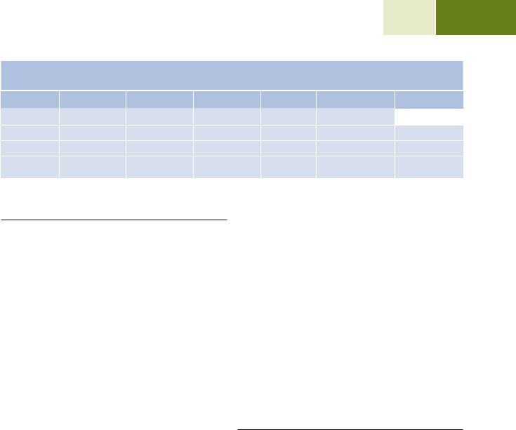
The monotonic dependence of electron backscattering upon atomic number (η vs. Z, shown in . Fig. 2.3) constitutes a number effect with predictable behavior that enables SEM imaging to reveal the compositional microstructure of a specimen through the contrast mechanism variously known as “atomic number contrast,” “compositional contrast,” “material contrast,” or “Z-contrast.” Ideally, to observe unobscured atomic number contrast, the specimen should be flat so that topography does not independently modify electron backscattering. An example of atomic number contrast observed in a polished cross section of Raney nickel alloy using signal collected with a semiconductor backscattered electron (BSE) detector is shown in . Fig. 7.1, where four regions with progressively higher gray levels can be identified. The systematic behavior of η versus Z allows the observer to confidently conclude that the average atomic number of these four regions increases as the average gray level increases. SEM/EDS microanalysis of these regions presented in . Table 7.1 gives the compositional results and calculated average atomic number, Zav, of each phase. The Zav values correspond to the trend of the gray levels of the phases observed in . Fig. 7.1.
. Fig. 7.1 Raney nickel; E0 = 20 keV; semiconductor BSE detector (SUM mode)
1
2
3
3
4
20 µm
113 |
7 |
7.2 · Interpretation of SEM Images of Compositional Microstructure
. Table 7.1 Raney nickel alloy (measured composition, calculated average atomic number, backscatter coefficient, and atomic number
contrast across the boundary between adjacent phases)
Phase |
Al (mass frac) |
Fe (mass frac) |
Ni (mass frac) |
Zav |
Calculated, η |
Contrast |
1 |
0.9874 |
0.0003 |
0.0123 |
13.2 |
0.155 |
|
|
|
|
|
|
|
|
2 |
0.6824 |
0.0409 |
0.2768 |
17.7 |
0.204 |
1–2 0.24 |
3 |
0.5817 |
0.0026 |
0.4155 |
19.3 |
0.22 |
2–3 0.073 |
4 |
0.4192 |
0.0007 |
0.5801 |
21.7 |
0.243 |
3–4 0.095 |
7.2.2\ Calculating Atomic Number Contrast
An SEM is typically equipped with a “dedicated backscattered electron detector” (e.g., semiconductor or passive scintillator) that produces a signal, S, proportional to the number of BSEs that strike it and thus to the backscattered electron coefficient, η, of the specimen. Note that other factors, such as the energy distribution of the BSEs, can also influence the detector response.
If the detector responded only to the number of BSEs, the contrast Ctr, can be estimated as
Ctr = (Smax − Smin ) / Smax = (hmax − hmin ) / hmax |
\ |
(7.2) |
|
|
Values of the backscatter coefficient for E0 ≥10 keV can be conveniently estimated using the fit to η versus Z (Eq. 2.2). Note that for mixtures that are uniform at the atomic level (e.g., alloy solid solutions, compounds, glasses, etc.), the backscattered electron coefficient can be calculated from the mass fraction average of the atomic number inserted into Eq. 2.2 (as illustrated for the Al-Fe-Ni phases listed in . Table 7.1), or alternatively, from the mass fraction average of the pure element backscatter coefficients.
The greater the difference in atomic number between two materials, the greater is the atomic number contrast. Consider two elements with a significant difference in atomic number, for example, Al (Z = 13, η = 0.152) and Cu (Z = 29, η = 0.302). From Eq. (7.1), the atomic number contrast between Al and Cu is estimated to be
Ctr = (hmax − hmin ) / hmax |
|
|
= (0.302 − 0.152) / 0.302 = 0.497 |
\ |
(7.3) |
|
|
When the contrast is calculated between elements separated by one unit of atomic number, much lower values are found, which has an important consequence on establishing visibility, as discussed below. Note that the slope of η versus Z decreases as Z increases, so that the contrast (which is the slope of η vs. Z) between adjacent elements ( Z = 1) also decreases. For example, the contrast between Al (Z = 13, η = 0.152) and Si (Z = 14, η = 0.164) where the slope of η versus Z is relatively high is
Ctr = (hmax − hmin ) / hmax |
|
|
= (0.164 − 0.152) / 0.164 = 0.073 |
\ |
(7.4) |
|
|
A similar calculation for Cu (Z = 29, η = 0.302) and Zn (Z = 30,
η = 0.310) where the slope of η versus Z is lower gives
Ctr = (0.310 − 0.302) / 0.310 = 0.026 |
\ |
(7.5) |
|
|
For high atomic number elements, the slope of η versus Z approaches zero, so that a calculation for Pt (Z = 78, η = 0.484) and Au (Z = 79, η = 0.487) gives a very low contrast:
Ctr = (0.487 − 0.484) / 0.487 = 0.0062 |
\ |
(7.6) |
|
|
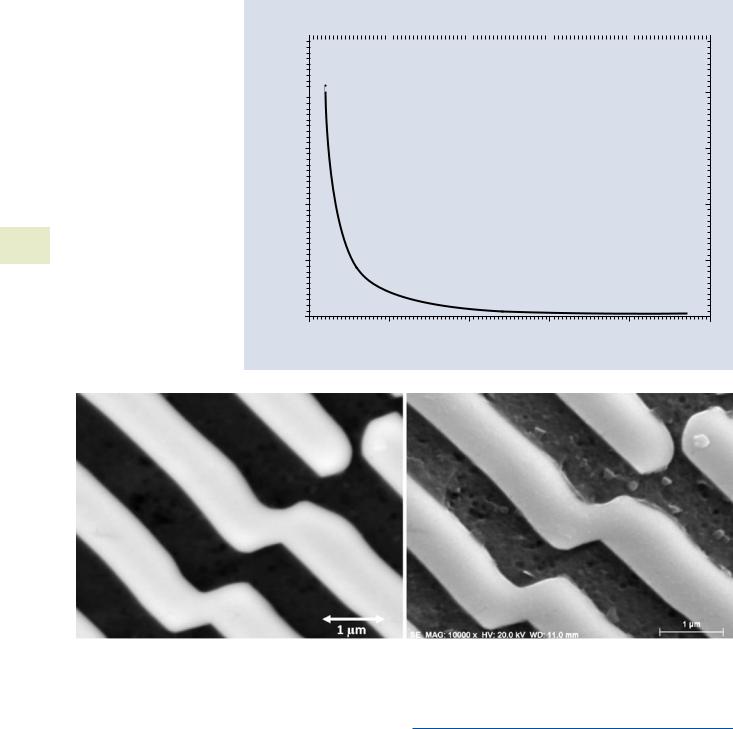
. Figure 7.2 summarizes this behavior in a plot of the BSE atomic number contrast for a unit change in Z as a function of Z.
7.2.3\ BSE Atomic Number Contrast
With the Everhart–Thornley Detector
The appearance of atomic number contrast for a polished cross section of Al-Cu aligned eutectic, which consists of an Al-2% Cu solid solution and the intermetallic CuAl2, is shown as viewed with a semiconductor BSE detector in . Fig. 7.3a and an Everhart–Thornley detector (positively biased) in . Fig. 7.3b. The E–T detector is usually thought of as a secondary electron detector, and while it captures the SE1 signal, it also captures BSEs that are directly emitted into the solid angle defined by the scintillator. Additionally, BSEs are also represented in the E–T detector signal by the large contribution of SE2 and SE3, which are actually BSE-modulated signals. Thus, although the SE1 signal of the E–T detector does not show predictable variation with composition, the BSE components of the E–T signal reveal the atomic number contrast seen in . Fig. 7.3b. It must be noted, however, that because of the sensitivity of the E–T detector to edge effects and topography, these fine-scale features are much more visible in . Fig. 7.3b than in . Fig. 7.3a.
For both the dedicated semiconductor BSE detector and the E–T detector, the higher atomic number regions appear brighter than the lower atomic number regions, as independently confirmed by energy dispersive X-ray spectrometry of both materials. However, the semiconductor BSE detector
\114 Chapter 7 · SEM Image Interpretation
. Fig. 7.2 Atomic number |
|
|
|
|
|
|
|
|
|
|
|
contrast for pure elements with |
|
|
|
|
Atomic number contrast for Z = 1 |
||||||
Z = 1 |
|
|
|
|
|||||||
0.5 |
|
|
|
|
|
|
|
|
|
|
|
|
|
|
|
|
|
|
|
|
|
|
|
|
0.4 |
|
|
|
|
|
|
|
|
|
|
|
|
|
|
|
|
|
|
|
|
|
|
Contrast
0.3
0.2
7
0.1
0.0
0 |
20 |
40 |
60 |
80 |
100 |
|
|
Atomic number |
|
|
|
a |
|
b |
|
|
|
. Fig. 7.3 Aligned Al-Cu eutectic; E0 = 20 keV: a semiconductor BSE detector (SUM mode); b Everhart–Thornley detector (positive bias)
actually enhances the atomic number contrast over that estimated from the composition (Al-0.02Cu, η = 0.155; CuAl2, η = 0.232, which gives Ctr = 0.33). The semiconductor detector shows increased response from higher energy backscattered electrons, which are produced in greater relative abundance from Cu compared to Al, thus enhancing the difference in the measured signals. The response of the Everhart- Thornley detector (positive bias) to BSEs is more complex. The BSEs that directly strike the scintillator produce a greater response with increasing energy. However, this component is small compared to the BSEs that strike the objective lens pole piece and chamber walls, where they are converted to SE3 and subsequently collected. For these remote BSEs, the lower energy fraction actually create SEs more efficiently.
7.3\ Interpretation of SEM Images
of Specimen Topography
Imaging the topographic features of specimens is one of the most important applications of the SEM, enabling the microscopist to gain information on size and shape of features. Topographic contrast has several components arising from both backscattered electrons and secondary electrons: \1.\ The backscattered electron coefficient shows a strong
dependence on the surface inclination, η versus θ. This effect contributes a number component to the observed contrast.
\2.\ Backscattering from a surface perpendicular to the beam (i.e., 0° tilt) is directional and follows a cosine
7.3 · Interpretation of SEM Images of Specimen Topography
distribution η(φ) ≈cos φ (where φ is an angle measured from the surface normal) that is rotationally symmetric around the beam. This effect contributes a trajectory component of contrast.
\3.\ Backscattering from a surface tilted to an angle θ becomes more highly directional and asymmetrical as θ increases, tending to peak in the forward scattering direction. This effect contributes a trajectory component of contrast.
\4.\ The secondary electron coefficient δ is strongly dependent on the surface inclination, δ(θ) ≈sec θ, increasing rapidly as the beam approaches grazing incidence. This effect contributes a number component of contrast.
Imaging of topography should be regarded as qualitative in nature because the details of the image such as shading depend not only on the specimen characteristics but also upon the response of the particular electron detector as well as its location and solid angle of acceptance. Nevertheless, the interpretation of all SEM images of topography is based on two principles regardless of the detector being used:
\1.\ Observer’s Point-of-View: The microscopist views the specimen features as if looking along the electron beam.
\2.\ Apparent Illumination of the Scene:
\a.\ The apparent major source of lighting of the scene comes from the position of the electron detector.
\b.\ Depending on the detector used, there may appear to be minor illumination sources coming from other directions.
115 7
7.3.1\ Imaging Specimen Topography
With the Everhart–Thornley Detector
SEM images of specimen topography collected with the Everhart–Thornley (positive bias) detector (Everhart and Thornley 1960) are surprisingly easy to interpret, considering how drastically the imaging technique differs from ordinary human visual experience: A finely focused electron beam steps sequentially through a series of locations on the specimen and a mixture of the backscattered electron and secondary electron signals, subject to the four number and trajectory effects noted above that result from complex beam–specimen interactions, is used to create the gray-scale image on the display. Nevertheless, a completely untrained observer (even a young child) can be reasonably expected to intuitively understand the general shape of a three-dimensional object from the details of the pattern of highlights and shading in the SEM/E–T (positive bias) image.
In fact, the appearance of a three-dimensional object viewed in an SEM/E–T (positive bias) image is strikingly similar to the view that would be obtained if that object were viewed with a conventional light source and the human eye, producing the socalled “light-optical analogy.” This situation is quite remarkable, and the relative ease with which SEM/E–T (positive bias) images can be utilized is a major source of the utility and popularity of the SEM. It is important to understand the origin of this SEM/E–T (positive bias) light-optical analogy and what pathological effects can occur to diminish or destroy the effect, possibly leading to incorrect image interpretation of topography.
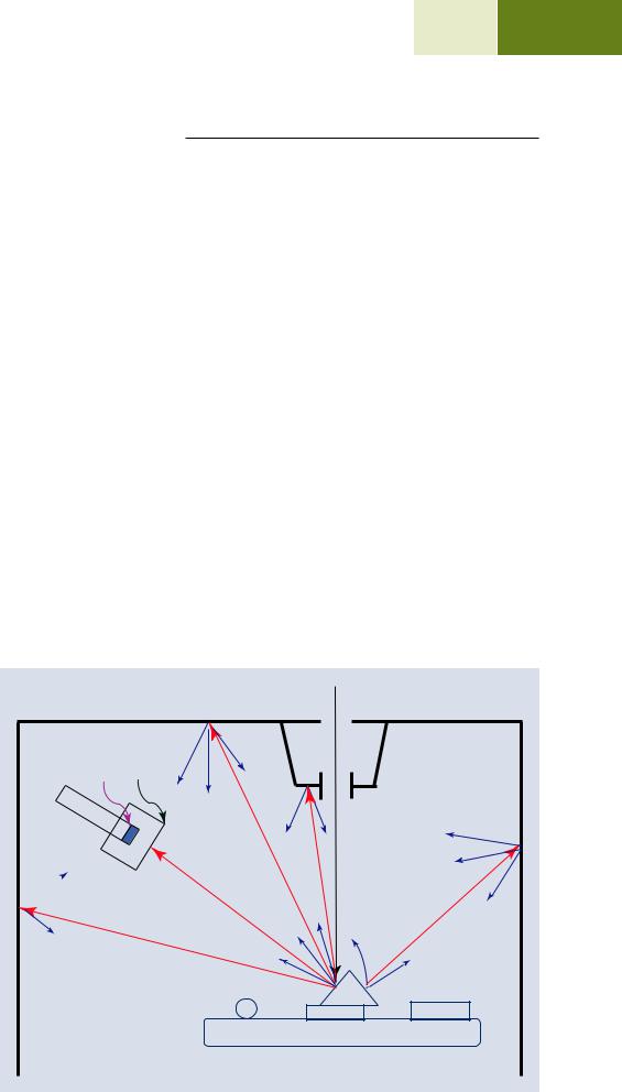
The E–T detector is mounted on the wall of the SEM specimen chamber asymmetrically off the beam axis, as illustrated schematically in . Fig. 7.4. The interaction of the beam
. Fig. 7.4 Schematic illustration of the various sources of signals generated from topography: BSEs, SE1 and SE2, and remote SE3 and collection by the Everhart– Thornley detector
+10 kV +300 V
SE3
SE3
SE3
 SE3
SE3
BSE
SE1,2 BSE
SE1,2
A B
C
\116 Chapter 7 · SEM Image Interpretation
with the specimen results in backscattering of beam electrons and secondary electron emission (type SE1 produced by the beam electrons entering the specimen and type SE2 produced by the exiting BSEs). Energetic BSEs carrying at least a few kilo-electronvolts of kinetic energy that directly strike the E–T scintillator are always detected, even if the scintillator is passive with no positive accelerating potential applied. In typical operation the E–T detector is operated with a large positive accelerating potential (+10 kV or higher) on the scintillator and a small positive bias (e.g., +300 V) on the Faraday cage which surrounds the scintillator. The small positive bias on the cage attracts SEs with high efficiency to the detector. Once they pass inside the Faraday cage, the SEs are accelerated to detectable kinetic energy by the high positive potential applied to the face of the scintillator. In addi-
7 tion to the SE1 and SE2 signals produced at the specimen, the E–T (positive bias) detector also collects some of the remotely produced SE3 which are generated where the BSEs strike the objective lens and the walls of the specimen chamber. Thus, in . Fig. 7.4 a feature such as face “A,” which is tilted toward the E–T detector, scatters some BSEs directly to the scintillator, which add to the SE1, SE2, and SE3 signals that are also collected, making “A” appear especially bright compared to face “B.” Because “B” is tilted away from the E–T (positive bias) detector, it does not make a direct BSE contribution, but some SE1 and SE2 signals will be collected from “B” by the Faraday cage potential, which causes SEs to follow curving trajectories, while remote SE3 signals from face “B” will also be collected. Only features the electron beam does not directly strike, such as the re-entrant feature “C,” will fail to generate any collectable signal and thus appear black.
7.3.2\ The Light-Optical Analogy to the SEM/ E–T (Positive Bias) Image
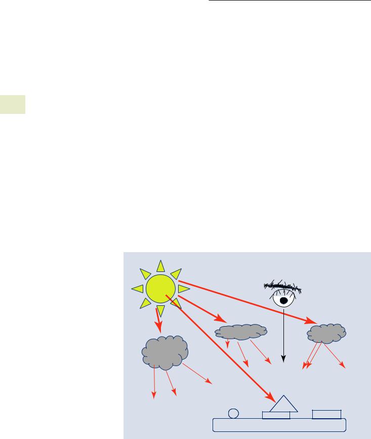
The complex mix of direct BSEs, SE1 and SE2, and remote SE3 illustrated in . Fig. 7.4 effectively illuminates the specimen in a way similar to the “real world” landscape scene illustrated schematically in . Fig. 7.5 (Oatley 1972). A viewer in an airplane looks down on a hilly landscape that is directionally illuminated by the Sun at a shallow (oblique) angle, highlighting sloping hillsides such as “A,” while a general pattern of diffuse light originates from scattering of sunlight by clouds and the atmosphere that illuminates all features, including those not in the direct path of the sunlight, such as hillside “B,” while the cave “C” receives no illumination. To establish this light-optical analogy, we must match components with similar characteristics:
\1.\ The human observer’s eye, which has a very sharply defined line-of-sight, is matched in characteristic by the electron beam, which presents a very narrow cone angle of rays: thus, the observer of an SEM image is effectively looking along the beam, and what the beam can strike is what can be observed in an image.
\2.\ The illumination of an outdoor scene by the Sun consists of a direct component (direct rays that strongly light those surfaces that they strike) and an indirect component (diffuse scattering of the Sun’s rays from clouds and the atmosphere, weakly illuminating the scene from all angles). For the E–T detector (positive bias), there is a direct signal component that acts like the Sun (BSEs emitted by the specimen into the solid angle defined by the scintillator, as well as SE1 and SE2 directly collected
. Fig. 7.5 Human visual experience equivalent to the observer position and lighting situation of the Everhart–Thornley (positive
bias) detector
Observer looking down on scene from vantage point directly above.
A B
C