


XV
Contents
1\ |
Electron Beam—Specimen Interactions: Interaction Volume |
|
1 |
|||||
1.1\ |
What |
Happens When the Beam Electrons Encounter Specimen Atoms? |
|
2 |
||||
1.2\ |
Inelastic |
Scattering (Energy Loss) Limits Beam Electron |
|
|
||||
|
Travel in the Specimen\ ........................... |
2 |
||||||
1.3\ |
Elastic |
Scattering: Beam Electrons Change Direction of Flight\ |
|
4 |
||||
1.3.1\ |
How |
Frequently Does Elastic Scattering Occur?\ |
|
4 |
||||
1.4\ |
Simulating |
the Effects of Elastic Scattering: Monte Carlo Calculations |
|
5 |
||||
1.4.1\ |
What |
Do Individual Monte Carlo Trajectories Look Like?\ |
|
6 |
||||
1.4.2\ |
Monte |
Carlo Simulation To Visualize the Electron Interaction Volume\ |
|
6 |
||||
1.4.3\ |
Using |
the Monte Carlo Electron Trajectory Simulation to Study |
|
|
||||
|
the Interaction Volume\ ............................ |
8 |
||||||
1.5\ |
A Range Equation To Estimate the Size of the Interaction Volume\ |
|
12 |
|||||
\ |
References .................................................. |
14 |
||||||
2\ |
Backscattered Electrons .. |
15 |
||||||
2.1Origin\ ............................................................ 16
2.1.1\ The Numerical Measure of Backscattered Electrons 16 2.2\ Critical Properties of Backscattered Electrons\ 16 2.2.1\ BSE Response to Specimen Composition (η vs. Atomic Number, Z)\ 16 2.2.2\ BSE Response to Specimen Inclination (η vs. Surface Tilt, θ)\ 20 2.2.3\ Angular Distribution of Backscattering\ 22 2.2.4\ Spatial Distribution of Backscattering . 23 2.2.5\ Energy Distribution of Backscattered Electrons\ 27
2.3Summary ...................................................... 27
\References .................................................... 28
3\ |
Secondary Electrons\ ......... 29 |
3.1Origin\ ............................................................ 30
3.2Energy Distribution\ ................................. 30
3.3\ |
Escape Depth of Secondary Electrons |
30 |
3.4\ |
Secondary Electron Yield Versus Atomic Number\ |
30 |
3.5 |
Secondary Electron Yield Versus Specimen Tilt\ |
34 |
3.6\ |
Angular Distribution of Secondary Electrons |
34 |
3.7\ |
Secondary Electron Yield Versus Beam Energy |
35 |
3.8\ |
Spatial Characteristics of Secondary Electrons |
35 |
\References .................................................... 37
4\ |
X-Rays ...................................... |
39 |
4.1 |
Overview ...................................................... |
40 |
4.2Characteristic X-Rays ............................... 40
4.2.1Origin\............................................................. 40
4.2.2Fluorescence Yield\..................................... 41
4.2.3 X-Ray Families\ 42
4.2.4X-Ray Nomenclature\ ................................. 43
4.2.5X-Ray Weights ofLines\ ............................. 44 4.2.6\ Characteristic X-Ray Intensity\ ................ 44
4.3 |
X-Ray Continuum (bremsstrahlung) ... 47 |
|||
4.3.1\ |
X-Ray Continuum Intensity ..................... 49 |
|||
4.3.2\ |
The |
Electron-Excited X-Ray Spectrum, As-Generated |
49 |
|
4.3.3\ |
Range |
of X-ray Production\...................... 50 |
||
4.3.4\ |
Monte |
Carlo Simulation of X-Ray Generation |
51 |
|
4.3.5\ |
X-ray Depth Distribution Function, ϕ(ρz) |
53 |
||
XVI\ Contents
4.4 X-Ray Absorption 54
4.5X-Ray Fluorescence\.................................. 59
\References .................................................... 63
5\ |
Scanning Electron Microscope (SEM) Instrumentation |
65 |
5.1Electron Beam Parameters .................... 66
5.2Electron Optical Parameters ................. 66
5.2.1Beam Energy\ ............................................... 66
5.2.2 |
Beam Diameter |
67 |
||
5.2.3 |
Beam Current\ |
67 |
||
5.2.4\ |
Beam |
Current Density\ .............................. 68 |
||
5.2.5\ |
Beam |
Convergence Angle, α\ .................. 68 |
||
5.2.6\ |
Beam |
Solid Angle |
69 |
|
5.2.7\ |
Electron |
Optical Brightness, β ................ 70 |
||
5.2.8Focus .............................................................. 71
5.3 SEM Imaging Modes\................................ 75 5.3.1\ High Depth-of-Field Mode ...................... 75
5.3.2High-Current Mode\................................... 78
5.3.3 Resolution Mode 80
5.3.4Low-Voltage Mode\ .................................... 81
5.4Electron Detectors\ ................................... 83
5.4.1\ Important Properties of BSE and SE for Detector Design and Operation 83
5.4.2Detector Characteristics\ .......................... 83
5.4.3\ |
Common |
Types of Electron Detectors\ |
85 |
||
5.4.4\ |
Secondary |
Electron Detectors\ ............... 86 |
|||
5.4.5\ |
Specimen |
Current: The Specimen as Its Own Detector\ |
88 |
||
5.4.6\ A Useful, Practical Measure of a Detector: Detective |
|
||||
|
Quantum Efficiency ................................... 89 |
||||
\References .................................................... 91
6\ |
Image Formation\ |
93 |
6.1\ |
Image Construction by Scanning Action |
94 |
6.2 |
Magnification\ |
95 |
6.2.1\ |
Magnification, Image Dimensions, and Scale Bars |
95 |
6.3Making Dimensional Measurements WiththeSEM:
How Big Is That Feature? ........................ 95
6.3.1Calibrating theImage ............................... 95
6.4 |
Image Defects\ |
98 |
||
6.4.1\ |
Projection |
Distortion (Foreshortening)\ |
98 |
|
6.4.2\ |
Image |
Defocusing (Blurring)\................ 100 |
||
6.5Making Measurements onSurfaces WithArbitrary Topography: Stereomicroscopy ................................... 102
6.5.1Qualitative Stereomicroscopy\ ............. 103
6.5.2Quantitative Stereomicroscopy\ .......... 107
\References .................................................. 110
7\ |
SEM Image Interpretation\ |
111 |
7.1Information inSEM Images \ ................ 112
7.2\ |
Interpretation of SEM Images of Compositional Microstructure |
112 |
||
7.2.1\ |
Atomic Number Contrast With Backscattered Electrons |
112 |
||
7.2.2\ |
Calculating Atomic Number Contrast\ |
113 |
||
7.2.3\ |
BSE Atomic Number Contrast With the Everhart–Thornley Detector\ |
113 |
||
7.3\ |
Interpretation of SEM Images of Specimen Topography\ |
114 |
||
7.3.1\ |
Imaging |
Specimen Topography With the Everhart–Thornley Detector\ |
115 |
|
7.3.2\ |
The |
Light-Optical Analogy to the SEM/E–T (Positive Bias) Image\ |
116 |
|
7.3.3\ |
Imaging |
Specimen Topography With a Semiconductor BSE Detector\ |
119 |
|
\ |
References .................................................. 121 |
|||

XVII
Contents
8\ |
The Visibility of Features in SEM Images\ |
123 |
8.1\ |
Signal Quality: Threshold Contrast and Threshold Current\ |
124 |
\References .................................................. 131
9\ |
Image Defects\.................... 133 |
||||
9.1 |
Charging\ .................................................... 134 |
||||
9.1.1\ |
What |
Is Specimen Charging?\ ............... 134 |
|||
9.1.2\ |
Recognizing |
Charging Phenomena in SEM Images |
135 |
||
9.1.3\ |
Techniques |
to Control Charging Artifacts (High Vacuum Instruments)\ |
139 |
||
9.2Radiation Damage\ ................................. 142
9.3 |
Contamination |
143 |
9.4\ |
Moiré Effects: Imaging What Isn’t Actually There |
144 |
\References .................................................. 146
10\ |
High Resolution Imaging |
147 |
10.1\ What Is “High Resolution SEM Imaging”? |
148 |
|
10.2Instrumentation Considerations\ ...... 148
10.3\ |
Pixel |
Size, Beam Footprint, and Delocalized Signals\ |
148 |
||||||||
10.4\ |
Secondary |
Electron Contrast at High Spatial Resolution |
150 |
||||||||
10.4.1\ |
SE |
range Effects Produce Bright Edges (Isolated Edges)\ |
151 |
||||||||
10.4.2\ |
Even |
More Localized Signal: Edges Which Are Thin Relative |
152 |
||||||||
|
to the Beam Range\ |
||||||||||
10.4.3\ |
Too |
Much of a Good Thing: The Bright Edge Effect Can Hinder |
|
||||||||
|
Distinguishing Shape\ ............................. 153 |
||||||||||
10.4.4\ |
Too |
Much of a Good Thing: The Bright Edge Effect Hinders |
154 |
||||||||
|
Locating the True Position of an Edge for Critical Dimension Metrology |
||||||||||
10.5\ |
Achieving |
High Resolution with Secondary Electrons |
156 |
||||||||
10.5.1\ |
Beam |
Energy Strategies\......................... 156 |
|||||||||
10.5.2 |
Improving theSE 1 Signal\....................... 158 |
||||||||||
10.5.3\ |
Eliminate |
the Use of SEs Altogether: “Low Loss BSEs“ |
161 |
||||||||
10.6\ |
Factors |
That Hinder Achieving High Resolution |
163 |
||||||||
10.6.1 |
Achieving Visibility: TheThreshold Contrast |
163 |
|||||||||
10.6.2\ |
Pathological |
Specimen Behavior\ ........ 163 |
|||||||||
10.6.3\ |
Pathological |
Specimen and Instrumentation Behavior |
164 |
||||||||
\References .................................................. 164
11\ |
Low Beam Energy SEM ... 165 |
|||||
11.1\ |
What |
Constitutes “Low” Beam Energy SEM Imaging?\ |
166 |
|||
11.2\ |
Secondary |
Electron and Backscattered Electron Signal Characteristics |
|
|||
|
in the Low Beam Energy Range\ ........ 166 |
|||||
11.3\ |
Selecting |
the Beam Energy to Control the Spatial Sampling |
|
|||
|
of Imaging Signals\ ................................. 169 |
|||||
11.3.1\ |
Low |
Beam Energy for High Lateral Resolution SEM |
169 |
|||
11.3.2\ |
Low |
Beam Energy for High Depth Resolution SEM |
169 |
|||
11.3.3\ |
Extremely |
Low Beam Energy Imaging\ |
171 |
|||
\References .................................................. 172
12\ |
Variable Pressure Scanning Electron Microscopy (VPSEM) |
173 |
|||
12.1\ |
Review: |
The Conventional SEM High Vacuum Environment |
174 |
||
12.1.1\ |
Stable |
Electron Source Operation\ ...... 174 |
|||
12.1.2 |
Maintaining Beam Integrity .................. 174 |
||||
12.1.3\ |
Stable |
Operation of the Everhart–Thornley Secondary Electron Detector\ |
174 |
||
12.1.4 |
Minimizing Contamination ................... 174 |
||||
12.2\ |
How |
Does VPSEM Differ From the Conventional SEM |
|
||
|
Vacuum Environment?\ ......................... 174 |
||||
\XVIII Contents
12.3\ |
Benefits |
of Scanning Electron Microscopy at Elevated Pressures |
175 |
|
12.3.1 |
Control ofSpecimen Charging\ ............ 175 |
|||
12.3.2\ |
Controlling |
the Water Environment of a Specimen\ |
176 |
|
12.4\ |
Gas Scattering Modification of the Focused Electron Beam |
177 |
||
12.5VPSEM Image Resolution\ .................... 181
12.6\ |
Detectors for Elevated Pressure Microscopy\ |
182 |
||
12.6.1\ |
Backscattered |
Electrons—Passive Scintillator Detector |
182 |
|
12.6.2\ |
Secondary |
Electrons–Gas Amplification Detector\ |
182 |
|
12.7Contrast inVPSEM\.................................. 184
\References .................................................. 185
13\ |
ImageJ and Fiji\ |
187 |
13.1The ImageJ Universe\ ............................. 188
13.2Fiji\ ................................................................. 188
13.3Plugins\ ........................................................ 190
13.4Where toLearn More ............................. 191
\References .................................................. 193
14\ |
SEM Imaging Checklist\ .. 195 |
||
14.1\ |
Specimen Considerations (High Vacuum SEM; Specimen Chamber Pressure < 10−3 Pa)\ |
197 |
|
14.1.1\ |
Conducting |
or Semiconducting Specimens\ |
197 |
14.1.2 |
Insulating Specimens\ ............................. 197 |
||
14.2Electron Signals Available ................... 197
14.2.1Beam Electron Range\ ............................. 197
14.2.2Backscattered Electrons ........................ 197
14.2.3Secondary Electrons \ .............................. 197
14.3Selecting theElectron Detector ........ 198
14.3.1\ Everhart–Thornley Detector (“Secondary Electron” Detector)\ 198
14.3.2Backscattered Electron Detectors\ ...... 198
14.3.3“Through-the-Lens” Detectors ............. 198
14.4\ |
Selecting the Beam Energy for SEM Imaging\ |
198 |
|
14.4.1 |
Compositional Contrast WithBackscattered Electrons\ |
198 |
|
14.4.2 |
Topographic Contrast WithBackscattered Electrons\ |
198 |
|
14.4.3 |
Topographic Contrast WithSecondary Electrons |
198 |
|
14.4.4\ |
High |
Resolution SEM Imaging\ ............. 198 |
|
14.5Selecting theBeam Current \ ............... 199
14.5.1 |
High Resolution Imaging\ ...................... 199 |
||
14.5.2\ |
Low |
Contrast Features Require High Beam Current and/or Long Frame Time to Establish Visibility\ |
199 |
14.6Image Presentation\ ............................... 199
14.6.1“Live” Display Adjustments\ ................... 199
14.6.2Post-Collection Processing\ ................... 199
14.7Image Interpretation ............................. 199
14.7.1Observer’s Point ofView\........................ 199
14.7.2Direction ofIllumination\ ....................... 199
14.7.3Contrast Encoding\................................... 200
14.7.4\ Imaging Topography With the Everhart–Thornley Detector\ 200 14.7.5\ Annular BSE Detector (Semiconductor Sum Mode A + B and Passive Scintillator)\ 200 14.7.6\ Semiconductor BSE Detector Difference Mode, A−B\ 200 14.7.7\ Everhart–Thornley Detector, Negatively Biased to Reject SE\ 200 14.8\ Variable Pressure Scanning Electron Microscopy (VPSEM) 200
14.8.1VPSEM Advantages\ ................................. 200
14.8.2VPSEM Disadvantages ............................ 200
15\ |
SEM Case Studies\ ............. 201 |
|
15.1\ |
Case Study: How High Is That Feature Relative to Another? |
202 |
15.2\ |
Revealing Shallow Surface Relief\ ..... 204 |
|
15.3\ |
Case Study: Detecting Ink-Jet Printer Deposits\ |
206 |

XIX
Contents
16\ |
Energy Dispersive X-ray Spectrometry: Physical Principles and User-Selected |
|
|||
|
Parameters\.......................... 209 |
||||
16.1\ |
The |
Energy Dispersive Spectrometry (EDS) Process\ |
210 |
||
16.1.1\ |
The |
Principal EDS Artifact: Peak Broadening (EDS Resolution Function)\ |
210 |
||
16.1.2 |
Minor Artifacts: TheSi-Escape Peak\ ... 213 |
||||
16.1.3\ |
Minor |
Artifacts: Coincidence Peaks .... 213 |
|||
16.1.4\ |
Minor |
Artifacts: Si Absorption Edge and Si Internal Fluorescence Peak\ |
215 |
||
16.2\ |
“Best |
Practices” for Electron-Excited EDS Operation\ |
216 |
||
16.2.1 |
Operation oftheEDS System ............... |
216 |
|||
16.3\ |
Practical |
Aspects of Ensuring EDS Performance for a Quality |
|
||
|
Measurement Environment ................ 219 |
||||
16.3.1 |
Detector Geometry\ ................................. 219 |
||||
16.3.2 |
Process Time\ |
222 |
|||
16.3.3Optimal Working Distance .................... 222
16.3.4Detector Orientation\ .............................. 223
16.3.5Count Rate Linearity\ ............................... 225
16.3.6Energy Calibration Linearity ................. 226
16.3.7Other Items\................................................ 227
16.3.8\ |
Setting |
Up a Quality Control Program\ |
228 |
16.3.9 |
Purchasing anSDD\.................................. 230 |
||
\References .................................................. 234
17\ DTSA-II EDS Software\ ..... 235
17.1Getting Started WithNIST DTSA-II\ ... 236
17.1.1Motivation .................................................. 236
17.1.2Platform\ ...................................................... 236
17.1.3Overview\ .................................................... 236
17.1.4Design\ ......................................................... 237
17.1.5\ The Three -Leg Stool: Simulation, Quantification and Experiment Design\ 237 17.1.6 Introduction toFundamental Concepts 238
17.2Simulation inDTSA-II\ ............................ 245
17.2.1Introduction\ .............................................. 245
17.2.2Monte Carlo Simulation ......................... 245
17.2.3 |
Using theGUI ToPerform aSimulation\ |
247 |
17.2.4 |
Optional Tables |
262 |
\References .................................................. 264
18\ |
Qualitative Elemental Analysis by Energy Dispersive X-Ray Spectrometry\ |
265 |
||||||
18.1\ |
Quality |
Assurance Issues for Qualitative Analysis: EDS Calibration |
266 |
|||||
18.2\ |
Principles |
of Qualitative EDS Analysis\ |
266 |
|||||
18.2.1\ |
Critical |
Concepts From the Physics of Characteristic X-ray Generation |
266 |
|||||
|
and Propagation\ |
|||||||
18.2.2\ |
X-Ray Energy Database: Families of X-Rays\ |
269 |
||||||
18.2.3\ |
Artifacts |
of the EDS Detection Process\ |
269 |
|||||
18.3\ |
Performing |
Manual Qualitative Analysis |
275 |
|||||
18.3.1\ |
Why |
are Skills in Manual Qualitative Analysis Important? |
275 |
|||||
18.3.2\ |
Performing |
Manual Qualitative Analysis: Choosing the Instrument |
|
|||||
|
Operating Conditions ............................. 277 |
|||||||
18.4Identifying thePeaks\ ............................ 278
18.4.1 |
Employ theAvailable Software Tools\ |
278 |
||
18.4.2\ |
Identifying |
the Peaks: Major Constituents |
280 |
|
18.4.3\ |
Lower |
Photon Energy Region\ .............. 281 |
||
18.4.4\ |
Identifying |
the Peaks: Minor and Trace Constituents |
281 |
|
18.4.5 |
Checking Your Work\................................ 281 |
|||
18.5\ |
A Worked Example of Manual Peak Identification |
281 |
||
\ |
References .................................................. 287 |
|||
XX\ Contents
19\ |
Quantitative Analysis: From k-ratio to Composition |
289 |
19.1 |
What Is ak-ratio?\ |
290 |
19.2Uncertainties ink-ratios ....................... 291
19.3 Sets ofk-ratios\ 291 19.4\ Converting Sets of k-ratios Into Composition\ 292
19.5The Analytical Total ................................ 292
19.6 |
Normalization\ |
292 |
|
19.7 |
Other Ways toEstimate C Z |
293 |
|
19.7.1\ |
Oxygen |
by Assumed Stoichiometry\ .. 293 |
|
19.7.2Waters ofCrystallization\........................ 293
19.7.3Element by Difference\............................ 293
19.8Ways ofReporting Composition\....... 294
19.8.1 |
Mass Fraction\ ............................................ 294 |
||
19.8.2 |
Atomic Fraction\ |
294 |
|
19.8.3 |
Stoichiometry\ ........................................... 294 |
||
19.8.4 |
Oxide Fractions |
294 |
|
19.9\ |
The |
Accuracy of Quantitative Electron-Excited X-ray Microanalysis\ |
295 |
19.9.1Standards-Based k-ratio Protocol\ ....... 295
19.9.2“Standardless Analysis”\ .......................... 296 19.10\ Appendix\ ................................................... 298
19.10.1\The |
Need for Matrix Corrections To Achieve Quantitative Analysis\ |
298 |
19.10.2\The |
Physical Origin of Matrix Effects\ . 299 |
|
19.10.3 ZAF Factors inMicroanalysis\ ................ 299
\References .................................................. 307
20\ Quantitative Analysis: The SEM/EDS Elemental Microanalysis k-ratio
Procedure for Bulk Specimens, Step-by-Step 309 20.1\ Requirements Imposed on the Specimen and Standards\ 311
20.2Instrumentation Requirements\ ........ 311
20.2.1Choosing theEDS Parameters\ ............. 311
20.2.2Choosing theBeam Energy, E0\ ............ 313
20.2.3Measuring theBeam Current ............... 313
20.2.4Choosing theBeam Current\................. 314
20.3\ |
Examples of the k-ratio/Matrix Correction Protocol with DTSA II |
316 |
|
20.3.1\ |
Analysis |
of Major Constituents (C > 0.1 Mass Fraction) |
|
|
with Well-Resolved Peaks\...................... 316 |
||
20.3.2\ |
Analysis |
of Major Constituents (C > 0.1 Mass Fraction) |
|
|
with Severely Overlapping Peaks\ ....... 318 |
||
20.3.3\ |
Analysis |
of a Minor Constituent with Peak Overlap From |
|
aMajor Constituent\ ................................ 319
20.3.4Ba-Ti Interference inBaTiSi 3O9\ ............. 319 20.3.5\ Ba-Ti Interference: Major/Minor Constituent Interference in K2496
Microanalysis Glass\ ................................. 319 20.4\ The Need for an Iterative Qualitative and Quantitative
Analysis Strategy\ .................................... 319
20.4.1\ |
Analysis |
of a Complex Metal Alloy, IN100\ |
|
320 |
|
20.4.2 |
Analysis ofaStainless Steel\ .................. |
|
323 |
||
20.4.3\ |
Progressive |
Discovery: Repeated Qualitative–Quantitative Analysis |
|
|
|
|
Sequences\.................................................. |
324 |
|||
20.5Is theSpecimen Homogeneous?\ ...... 326
20.6Beam-Sensitive Specimens ................. 331
20.6.1 |
Alkali Element Migration\....................... 331 |
|
20.6.2\ |
Materials |
Subject to Mass Loss During Electron Bombardment— |
|
the Marshall-Hall Method\ ..................... 334 |
|
\ |
References .................................................. 339 |
|
XXI
Contents
21\ |
Trace Analysis by SEM/EDS\ |
341 |
21.1\ Limits of Detection for SEM/EDS Microanalysis 342 21.2\ Estimating the Concentration Limit of Detection, CDL\ 343
21.2.1Estimating CDL from a Trace or Minor Constituent from Measuring
a Known Standard\ ................................... 343
21.2.2Estimating CDL After Determination of a Minor or Trace Constituent
343with Severe Peak Interference from a Major Constituent\
21.2.3Estimating CDL When a Reference Value for Trace or
Minor Element Is Not Available\........... 343
21.3\ |
Measurements |
of Trace Constituents by Electron-Excited Energy |
|
||
|
Dispersive X-ray Spectrometry\ ......... 345 |
||||
21.3.1\ |
Is a Given Trace Level Measurement Actually Valid? |
345 |
|||
21.4\ |
Pathological |
Electron Scattering Can Produce “Trace” Contributions |
|
||
|
to EDS Spectra\ |
350 |
|||
21.4.1\ |
Instrumental |
Sources of Trace Analysis Artifacts\ |
350 |
||
21.4.2\ |
Assessing |
Remote Excitation Sources in an SEM-EDS System |
353 |
||
21.5Summary .................................................... 357
\References .................................................. 357
22\ |
Low Beam Energy X-Ray Microanalysis\ |
359 |
|||||||
22.1\ |
What |
Constitutes “Low” Beam Energy X-Ray Microanalysis? |
360 |
||||||
22.1.1\ |
Characteristic |
X-ray Peak Selection Strategy for Analysis\ |
364 |
||||||
22.1.2\ |
Low |
Beam Energy Analysis Range\...... 364 |
|||||||
22.2\ |
Advantage of Low Beam Energy X-Ray Microanalysis\ |
365 |
|||||||
22.2.1 |
Improved Spatial Resolution ................ 365 |
||||||||
22.2.2\ |
Reduced |
Matrix Absorption Correction |
366 |
||||||
22.2.3\ |
Accurate |
Analysis of Low Atomic Number Elements at Low Beam Energy |
366 |
||||||
22.3\ |
Challenges |
and Limitations of Low Beam Energy X-Ray Microanalysis\ |
369 |
||||||
22.3.1 |
Reduced Access toElements ................ 369 |
||||||||
22.3.2\ |
Relative |
Depth of X-Ray Generation: Susceptibility to Vertical Heterogeneity |
372 |
||||||
22.3.3\ |
At |
Low Beam Energy, Almost Everything Is Found To Be Layered\ |
373 |
||||||
\References\................................................. 380
23\ |
Analysis of Specimens with Special Geometry: Irregular Bulk |
|
||||||||
|
Objects and Particles |
381 |
||||||||
23.1\ |
The |
Origins of “Geometric Effects”: Bulk Specimens |
382 |
|||||||
23.2\ |
What |
Degree of Surface Finish Is Required for Electron-Excited X-ray |
|
|||||||
|
Microanalysis To Minimize Geometric Effects?\ |
384 |
||||||||
23.2.1 |
No Chemical Etching\ .............................. 384 |
|||||||||
23.3\ |
Consequences |
of Attempting Analysis of Bulk Materials |
|
|||||||
|
With Rough Surfaces\............................. 385 |
|||||||||
23.4\ |
Useful |
Indicators of Geometric Factors Impact on Analysis |
386 |
|||||||
23.4.1 |
The Raw Analytical Total\........................ 386 |
|||||||||
23.4.2\ |
The |
Shape of the EDS Spectrum\ ......... 389 |
||||||||
23.5\ |
Best |
Practices for Analysis of Rough Bulk Samples\ |
391 |
|||||||
23.6 |
Particle Analysis\ |
394 |
||||||||
23.6.1\ |
How |
Do X-ray Measurements of Particles Differ |
|
|||||||
|
From Bulk Measurements? .................... 394 |
|||||||||
23.6.2\ |
Collecting |
Optimum Spectra From Particles |
395 |
|||||||
23.6.3\ |
X-ray Spectrum Imaging: Understanding Heterogeneous Materials |
400 |
||||||||
23.6.4\ |
Particle |
Geometry Factors Influencing Quantitative Analysis of Particles |
403 |
|||||||
23.6.5\ |
Uncertainty |
in Quantitative Analysis of Particles\ |
405 |
|||||||
23.6.6 |
Peak-to-Background (P/B) Method\ .... 408 |
|||||||||
23.7Summary .................................................... 410
\ |
References .................................................. 411 |
\XXII Contents
24\ |
Compositional Mapping\ |
413 |
24.1\ Total Intensity Region-of-Interest Mapping 414 24.1.1\ Limitations of Total Intensity Mapping\ 415
24.2X-Ray Spectrum Imaging\..................... 417
24.2.1 |
Utilizing XSI Datacubes .......................... 419 |
|
24.2.2 |
Derived Spectra |
419 |
24.3 |
Quantitative Compositional Mapping |
424 |
24.4\ |
Strategy for XSI Elemental Mapping Data Collection |
430 |
24.4.1Choosing theEDS Dead-Time .............. 430
24.4.2Choosing thePixel Density ................... 432
24.4.3Choosing thePixel Dwell Time\ ............ 434
\References .................................................. 439
25\ |
Attempting Electron-Excited X-Ray Microanalysis in the Variable Pressure |
|
||
|
Scanning Electron Microscope (VPSEM)\ |
441 |
||
25.1\ |
Gas Scattering Effects in the VPSEM |
442 |
||
25.1.1\ |
Why |
Doesn’t the EDS Collimator Exclude the Remote Skirt X-Rays? |
446 |
|
25.1.2\ |
Other |
Artifacts Observed in VPSEM X-Ray Spectrometry\ |
448 |
|
25.2\ |
What Can Be Done To Minimize gas Scattering in VPSEM?\ |
450 |
||
25.2.1 |
Workarounds ToSolve Practical Problems |
451 |
||
25.2.2Favorable Sample Characteristics ....... 451
25.2.3Unfavorable Sample Characteristics .. 456
\References .................................................. 459
26\ |
Energy Dispersive X-Ray Microanalysis Checklist\ |
461 |
26.1 |
Instrumentation\ |
462 |
26.1.1SEM ............................................................... 462
26.1.2EDS Detector\ ............................................. 462 26.1.3\ Probe Current Measurement Device\ . 462
26.1.4 Conductive Coating\ ................................ 463
26.2Sample Preparation\............................... 463
26.2.1Standard Materials\ .................................. 464
26.2.2Peak Reference Materials\ ...................... 464
26.3Initial Set-Up ............................................. 464
26.3.1 |
Calibrating theEDS Detector\............... |
464 |
|
26.4 |
Collecting Data\ |
|
466 |
26.4.1Exploratory Spectrum\ ............................ 466
26.4.2Experiment Optimization ...................... 467
26.4.3Selecting Standards\ ................................ 467
26.4.4 Reference Spectra 467
26.4.5Collecting Standards\ .............................. 467
26.4.6Collecting Peak-Fitting References\ .... 467
26.4.7 |
Collecting Spectra FromtheUnknown\ |
467 |
|
26.5 |
Data Analysis |
468 |
|
26.5.1 |
Organizing theData ................................ 468 |
||
26.5.2 |
Quantification\ |
468 |
|
26.6 |
Quality Check\ |
468 |
|
26.6.1\ |
Check |
the Residual Spectrum After Peak Fitting\ |
468 |
26.6.2Check theAnalytic Total\ ........................ 469
26.6.3Intercompare theMeasurements\ ....... 469
\Reference .................................................... 470
27\ |
X-Ray Microanalysis Case Studies |
471 |
27.1\ |
Case Study: Characterization of a Hard-Facing Alloy Bearing Surface\ |
472 |
27.2\ |
Case Study: Aluminum Wire Failures in Residential Wiring |
474 |
27.3\ |
Case Study: Characterizing the Microstructure of a Manganese Nodule\ |
476 |
\ |
References .................................................. 479 |
|

XXIII
Contents
28\ |
Cathodoluminescence\ ... 481 |
28.1Origin\ .......................................................... 482
28.2Measuring Cathodoluminescence\ ... 483
28.2.1 |
Collection ofCL\ |
483 |
28.2.2 |
Detection ofCL |
483 |
28.3 |
Applications ofCL\ |
485 |
28.3.1 |
Geology ....................................................... 485 |
|
28.3.2 |
Materials Science\ |
485 |
28.3.3 |
Organic Compounds ............................... 489 |
|
\References .................................................. 489
29\ |
Characterizing Crystalline Materials in the SEM\ |
491 |
29.1\ Imaging Crystalline Materials with Electron Channeling Contrast\ |
492 |
|
29.1.1Single Crystals ........................................... 492
29.1.2Polycrystalline Materials\........................ 494
29.1.3\ |
Conditions |
for Detecting Electron Channeling Contrast\ |
496 |
|||
29.2\ |
Electron |
Backscatter Diffraction in the Scanning Electron |
|
|||
|
Microscope ................................................ 496 |
|||||
29.2.1 |
Origin ofEBSD Patterns\ ......................... 498 |
|||||
29.2.2\ |
Cameras |
for EBSD Pattern Detection . 499 |
||||
29.2.3 |
EBSD Spatial Resolution ......................... 499 |
|||||
29.2.4\ |
How |
Does a Modern EBSD System Index Patterns |
501 |
|||
29.2.5\ |
Steps |
in Typical EBSD Measurements |
502 |
|||
29.2.6Display oftheAcquired Data\ ............... 505
29.2.7Other Map Components ........................ 508
29.2.8\ Dangers and Practice of “Cleaning” EBSD Data\ 508 29.2.9\ Transmission Kikuchi Diffraction in the SEM 509
29.2.10Application Example ............................... 510
29.2.11Summary\ .................................................... 513
29.2.12\Electron Backscatter Diffraction Checklist\ 513
\References .................................................. 514
30\ |
Focused Ion Beam Applications in the SEM Laboratory\ |
517 |
|
30.1 |
Introduction\ |
518 |
|
30.2 |
Ion–Solid Interactions\ .......................... 518 |
||
30.3\ |
Focused |
Ion Beam Systems ................. 519 |
|
30.4 |
Imaging withIons |
520 |
|
30.5Preparation ofSamples forSEM\ ....... 521
30.5.1 |
Cross-Section Preparation\ .................... 522 |
||
30.5.2\ |
FIB |
Sample Preparation for 3D Techniques and Imaging |
524 |
30.6Summary .................................................... 526
\References .................................................. 528
31\ Ion Beam Microscopy\ ..... 529 31.1\ What Is So Useful About Ions?\........... 530
31.2Generating Ion Beams\ .......................... 533
31.3Signal Generation intheHIM ............. 534
31.4\ Current Generation and Data Collection in the HIM\ 536
31.5Patterning withIon Beams\ ................. 537
31.6Operating theHIM\ ................................. 538
31.7\ |
Chemical |
Microanalysis with Ion Beams |
538 |
\ |
References .................................................. 539 |
||
\ |
Supplementary Information\ |
541 |
|
|
Appendix\ .................................................... 542 |
||
\ |
Index\.......................................................... 547 |
||

1 |
|
1 |
|
|
|
Electron Beam—Specimen
Interactions: Interaction
Volume
1.1\ What Happens When the Beam Electrons Encounter Specimen Atoms? – 2
1.2\ Inelastic Scattering (Energy Loss) Limits Beam
Electron Travel in the Specimen – 2
1.3\ Elastic Scattering: Beam Electrons Change
Direction of Flight – 4
1.3.1\ How Frequently Does Elastic Scattering Occur? – 4
1.4\ Simulating the Effects of Elastic Scattering: Monte Carlo Calculations – 5
1.4.1\ What Do Individual Monte Carlo Trajectories Look Like? – 6 1.4.2\ Monte Carlo Simulation To Visualize the Electron
Interaction Volume – 6
1.4.3\ Using the Monte Carlo Electron Trajectory Simulation to Study the Interaction Volume – 8
1.5\ A Range Equation To Estimate the Size of the Interaction Volume – 12
\References – 14
© Springer Science+Business Media LLC 2018
J. Goldstein et al., Scanning Electron Microscopy and X-Ray Microanalysis, https://doi.org/10.1007/978-1-4939-6676-9_1

\2 Chapter 1 · Electron Beam—Specimen Interactions: Interaction Volume
1 |
1.1\ What Happens When the Beam |
Electrons Encounter Specimen Atoms? |
By selecting the operating parameters of the SEM electron gun, lenses, and apertures, the microscopist controls the characteristics of the focused beam that reaches the specimen surface: energy (typically selected in the range 0.1– 30 keV), diameter (0.5 nm to 1 μm or larger), beam current (1 pA to 1 μA), and convergence angle (semi-cone angle 0.001–0.05 rad). In a conventional high vacuum SEM (typically with the column and specimen chamber pressures reduced below 10−3 Pa), the residual atom density is so low that the beam electrons are statistically unlikely to encounter any atoms of the residual gas along the flight path from the electron source to the specimen, a distance of approximately 25 cm.
kThe initial dimensional scale
With a cold or thermal field emission gun on a highperformance SEM, the incident beam can be focused to 1 nm in diameter, which means that for a target such as gold (atom diameter ~ 288 pm), there are approximately 12 gold atoms in the first atomic layer of the solid within the area of the beam footprint at the surface.
At the specimen surface the atom density changes abruptly to the very high density of the solid. The beam electrons interact with the specimen atoms through a variety of physical processes collectively referred to as “scattering events.” The overall effects of these scattering events are to transfer energy to the specimen atoms from the beam electrons, thus setting a limit on their travel within the solid, and to alter the direction of travel of the beam electrons away from the well-defined incident beam trajectory. These beam electron–specimen interactions produce the backscattered electrons (BSE), secondary electrons (SE), and X-rays that convey information about the specimen, such as coarseand fine-scale topographic features, composition, crystal structure, and local electrical and magnetic fields. At the level needed to interpret SEM images and to perform electronexcited X-ray microanalysis, the complex variety of scattering processes will be broadly classified into “inelastic” and “elastic” scattering.
1.2\ Inelastic Scattering (Energy Loss)
Limits Beam Electron Travel
in the Specimen
“Inelastic” scattering refers to a variety of physical processes that act to progressively reduce the energy of the beam electron by transferring that energy to the specimen atoms through interactions with tightly bound inner-shell atomic electrons and loosely bound valence electrons. These energy loss processes include ejection of weakly bound outer-shell
atomic electrons (binding energy of a few eV) to form secondary electrons; ejection of tightly bound inner shell atomic electrons (binding energy of hundreds to thousands of eV) which subsequently results in emission of characteristic X-rays; deceleration of the beam electron in the electrical field of the atoms producing an X-ray continuum over all energies from a few eV up to the beam’s landing energy (E0) (bremsstrahlung or “braking radiation”); generation of waves in the free electron gas that permeates conducting metallic solids (plasmons); and heating of the specimen (phonon production). While energy is lost in these inelastic scattering events, the beam electrons only deviate slightly from their current path. The energy loss due to inelastic scattering sets an eventual limit on how far the beam electron can travel in the specimen before it loses all of its energy and is absorbed by the specimen.
To understand the specific limitations on the distance traveled in the specimen imposed by inelastic scattering, a mathematical description is needed of the rate of energy loss (incremental dE, measured in eV) with distance (incremental ds, measured in nm) traveled in the specimen. Although the various inelastic scattering energy loss processes are discrete and independent, Bethe (1930) was able to summarize their collective effects into a “continuous energy loss approximation”:
dE / ds (eV / nm) = − 7.85(Z r / AE)ln (1.166 E / J ) \ (1.1a)
where E is the beam energy (keV), Z is the atomic number, ρ is the density (g/cm3), A is the atomic weight (g/mol), and J is the “mean ionization potential” (keV) given by
J (keV)= (9.76 Z + 58.5 Z −0.19 )x10−3 |
\ |
(1.1b) |
|
|
The Bethe expression is plotted for several elements (C, Al, Cu, Ag, Au) over the range of “conventional” SEM operating energies, 5–30 keV in . Fig. 1.1. This figure reveals that the rate of energy loss dE/ds increases as the electron energy decreases and increases with the atomic number of the target. An electron with a beam energy of 20 keV loses energy at approximately 10 eV/nm in Au, so that if this rate was constant, the total path traveled in the specimen would be approximately 20,000 eV/(10 eV/nm) = 2000 nm = 2 μm. A better estimate of this electron “Bethe range” can be made by explicitly considering the energy dependence of dE/ds through integration of the Bethe expression, Eq. 1.1a, from the incident energy down to a lower cut-off energy (typically ~ 2 keV due to limitations on the range of applicability of the Bethe expression; see further discussion below). Based on this calculation, the Bethe range for the selection of elements is shown in . Fig. 1.2. At a particular incident beam energy, the Bethe range decreases as the atomic number of the target increases, while for a particular target, the Bethe range increases as the incident beam energy increases.
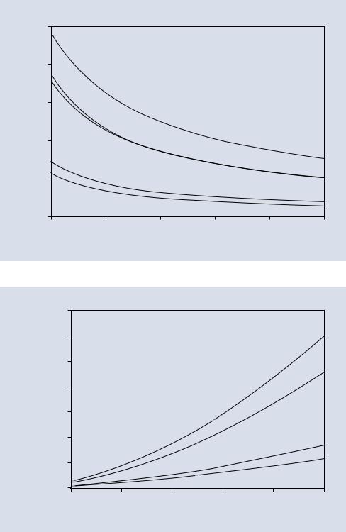
1.2 · Inelastic Scattering (Energy Loss) Limits Beam Electron Travel in the Specimen |
|
|||
. Fig. 1.1 Bethe continuous |
|
|
|
|
energy loss model calculations for |
|
|
Bethe continuous energy loss model |
|
dE/ds in C, Al, Cu, Ag, and Au as a |
|
|
||
25 |
|
|
|
|
function of electron energy |
|
|
|
|
|
|
|
|
|
|
|
Au |
|
|
(eV/nm) |
20 |
|
|
|
15 |
Ag |
|
|
|
|
|
|
|
|
rate |
|
Cu |
|
|
loss |
|
|
|
|
10 |
|
|
|
|
Energy |
|
|
|
|
|
Al |
|
|
|
|
|
|
|
|
|
5 |
|
|
|
|
|
C |
|
|
|
0 |
|
|
|
|
5 |
10 |
15 |
20 |
Incident beam energy (keV)
. Fig. 1.2 Bethe range calcula- |
|
|
|
|
|
tion from the continuous energy |
|
|
|
|
Bethe range |
loss model by integrating over the |
|
14000 |
|
|
|
range of energy from E0 down to a |
|
|
|
|
|
cut-off energy of 2 keV |
|
12000 |
|
|
|
|
|
|
|
|
|
|
|
10000 |
|
|
|
|
(nm) |
8000 |
|
|
|
|
range |
|
|
|
|
|
|
|
|
|
|
|
Bethe |
6000 |
|
|
|
|
|
|
|
|
|
|
|
4000 |
|
|
|
|
|
2000 |
|
|
|
|
|
0 |
|
|
|
|
|
5 |
10 |
15 |
20 |
Incident beam energy (keV)
3 |
|
1 |
|
|
|
25 |
30 |
C
Al
Cu, Ag
Au
25 30
kNote the change of scale
The Bethe range for Au with an incident beam energy of 20 keV is approximately 1200 nm, a linear change in scale of a factor of 1200 over an incident beam diameter of 1 nm. If the beam–specimen interactions were restricted to a cylindrical column with the circular beam entrance footprint as its
cross section and the Bethe range as its altitude, the volume of a cylinder 1 nm in diameter and 1200 nm deep would be approximately 940 nm3, and the number of gold atoms it contained would be approximately 7.5 × 10⁴, which can be compared to the incident beam footprint surface atom count of approximately 12.
\4 Chapter 1 · Electron Beam—Specimen Interactions: Interaction Volume
|
1.3\ Elastic Scattering: Beam Electrons |
|
|||||
1 |
|
||||||
|
|
Change Direction of Flight |
|
|
|
|
|
|
|
|
|||||
|
Simultaneously with inelastic scattering, “elastic scattering” |
||||||
|
events occur when the beam electron is deflected by the elec- |
||||||
|
trical field of an atom (the positive nuclear charge as partially |
||||||
|
shielded by the negative charge of the atom’s orbital elec- |
||||||
|
trons), causing the beam electron to deviate from its previous |
||||||
|
path onto a new trajectory, as illustrated schematically in |
||||||
|
. Fig. |
1.3a. The probability of elastic scattering depends |
|||||
|
strongly on the nuclear charge (atomic number Z) and the |
||||||
|
energy of the electron, E (keV) and is expressed mathemati- |
||||||
|
cally as a cross section, Q: |
|
|
|
|
||
|
|
Qelastic(>φ 0 ) =1.62×10⁻²⁰ (Z2 / E2 )cot2 (φ0 / 2) |
|
|
|
||
|
|
|
|
2 |
|
|
(1.2) |
|
|
|
[events > φ0 / electron (atom / cm |
|
) |
\ |
|
|
|
|
|
|
|
|
|
a
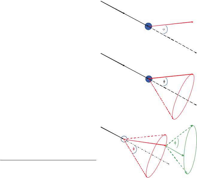
b
P1
P1
where ϕ0 is a threshold elastic scattering angle, for example, 2°. Despite the angular deviation, the beam electron energy is effectively unchanged in energy. While the average elastic scattering event causes an angular change of only a few degrees, deviations up to 180o are possible in a single elastic scattering event. Elastic scattering causes beam electrons to deviate out of the narrow angular range of incident trajectories defined by the convergence of the incident beam as controlled by the electron optics.
1.3.1\ How Frequently Does Elastic
Scattering Occur?
The elastic scattering cross section, Eq. 1.2, can be used to estimate how far the beam electron must travel on average to experience an elastic scattering event, a distance called the “mean free path,” λ:
λelastic (cm)= A / |
|
|
|
|
(1.3a) |
|
N0 ρQelastic(>φ 0 ) |
\ |
|
||||
λelastic (nm)=10 |
7 |
|
|
|
|
|
A / N0 |
ρQelastic(>φ 0 ) |
|
(1.3b) |
|||
|
\ |
|||||
|
|
|
|
|
|
|
c
P1
P2 
 P3
P3
. Fig. 1.3 a Schematic illustration of elastic scattering. An energetic electron is deflected by the electrical field of an atom at location P1
through an angle ϕelastic. b Schematic illustration of the elastic scattering cone. The energetic electron scatters elastically at point P1 and can
land at any location on the circumference of the base of the cone with equal probability. c Schematic illustration of a second scattering step, carrying the energetic electron from point P2 to point P3
where A is the atomic weight (g/mol), N0 is Avogadro’s number (atoms/mol), and ρ is the density (g/cm3). . Figure 1.4
shows a plot of λelastic for various elements as a function of electron energy, where it can be seen that the mean free path
is of the order of nm. Elastic scattering is thus likely to occur hundreds to thousands of times along a Bethe range of several hundred to several thousand nanometers.