

- •Preface
- •Imaging Microscopic Features
- •Measuring the Crystal Structure
- •References
- •Contents
- •1.4 Simulating the Effects of Elastic Scattering: Monte Carlo Calculations
- •What Are the Main Features of the Beam Electron Interaction Volume?
- •How Does the Interaction Volume Change with Composition?
- •How Does the Interaction Volume Change with Incident Beam Energy?
- •How Does the Interaction Volume Change with Specimen Tilt?
- •1.5 A Range Equation To Estimate the Size of the Interaction Volume
- •References
- •2: Backscattered Electrons
- •2.1 Origin
- •2.2.1 BSE Response to Specimen Composition (η vs. Atomic Number, Z)
- •SEM Image Contrast with BSE: “Atomic Number Contrast”
- •SEM Image Contrast: “BSE Topographic Contrast—Number Effects”
- •2.2.3 Angular Distribution of Backscattering
- •Beam Incident at an Acute Angle to the Specimen Surface (Specimen Tilt > 0°)
- •SEM Image Contrast: “BSE Topographic Contrast—Trajectory Effects”
- •2.2.4 Spatial Distribution of Backscattering
- •Depth Distribution of Backscattering
- •Radial Distribution of Backscattered Electrons
- •2.3 Summary
- •References
- •3: Secondary Electrons
- •3.1 Origin
- •3.2 Energy Distribution
- •3.3 Escape Depth of Secondary Electrons
- •3.8 Spatial Characteristics of Secondary Electrons
- •References
- •4: X-Rays
- •4.1 Overview
- •4.2 Characteristic X-Rays
- •4.2.1 Origin
- •4.2.2 Fluorescence Yield
- •4.2.3 X-Ray Families
- •4.2.4 X-Ray Nomenclature
- •4.2.6 Characteristic X-Ray Intensity
- •Isolated Atoms
- •X-Ray Production in Thin Foils
- •X-Ray Intensity Emitted from Thick, Solid Specimens
- •4.3 X-Ray Continuum (bremsstrahlung)
- •4.3.1 X-Ray Continuum Intensity
- •4.3.3 Range of X-ray Production
- •4.4 X-Ray Absorption
- •4.5 X-Ray Fluorescence
- •References
- •5.1 Electron Beam Parameters
- •5.2 Electron Optical Parameters
- •5.2.1 Beam Energy
- •Landing Energy
- •5.2.2 Beam Diameter
- •5.2.3 Beam Current
- •5.2.4 Beam Current Density
- •5.2.5 Beam Convergence Angle, α
- •5.2.6 Beam Solid Angle
- •5.2.7 Electron Optical Brightness, β
- •Brightness Equation
- •5.2.8 Focus
- •Astigmatism
- •5.3 SEM Imaging Modes
- •5.3.1 High Depth-of-Field Mode
- •5.3.2 High-Current Mode
- •5.3.3 Resolution Mode
- •5.3.4 Low-Voltage Mode
- •5.4 Electron Detectors
- •5.4.1 Important Properties of BSE and SE for Detector Design and Operation
- •Abundance
- •Angular Distribution
- •Kinetic Energy Response
- •5.4.2 Detector Characteristics
- •Angular Measures for Electron Detectors
- •Elevation (Take-Off) Angle, ψ, and Azimuthal Angle, ζ
- •Solid Angle, Ω
- •Energy Response
- •Bandwidth
- •5.4.3 Common Types of Electron Detectors
- •Backscattered Electrons
- •Passive Detectors
- •Scintillation Detectors
- •Semiconductor BSE Detectors
- •5.4.4 Secondary Electron Detectors
- •Everhart–Thornley Detector
- •Through-the-Lens (TTL) Electron Detectors
- •TTL SE Detector
- •TTL BSE Detector
- •Measuring the DQE: BSE Semiconductor Detector
- •References
- •6: Image Formation
- •6.1 Image Construction by Scanning Action
- •6.2 Magnification
- •6.3 Making Dimensional Measurements With the SEM: How Big Is That Feature?
- •Using a Calibrated Structure in ImageJ-Fiji
- •6.4 Image Defects
- •6.4.1 Projection Distortion (Foreshortening)
- •6.4.2 Image Defocusing (Blurring)
- •6.5 Making Measurements on Surfaces With Arbitrary Topography: Stereomicroscopy
- •6.5.1 Qualitative Stereomicroscopy
- •Fixed beam, Specimen Position Altered
- •Fixed Specimen, Beam Incidence Angle Changed
- •6.5.2 Quantitative Stereomicroscopy
- •Measuring a Simple Vertical Displacement
- •References
- •7: SEM Image Interpretation
- •7.1 Information in SEM Images
- •7.2.2 Calculating Atomic Number Contrast
- •Establishing a Robust Light-Optical Analogy
- •Getting It Wrong: Breaking the Light-Optical Analogy of the Everhart–Thornley (Positive Bias) Detector
- •Deconstructing the SEM/E–T Image of Topography
- •SUM Mode (A + B)
- •DIFFERENCE Mode (A−B)
- •References
- •References
- •9: Image Defects
- •9.1 Charging
- •9.1.1 What Is Specimen Charging?
- •9.1.3 Techniques to Control Charging Artifacts (High Vacuum Instruments)
- •Observing Uncoated Specimens
- •Coating an Insulating Specimen for Charge Dissipation
- •Choosing the Coating for Imaging Morphology
- •9.2 Radiation Damage
- •9.3 Contamination
- •References
- •10: High Resolution Imaging
- •10.2 Instrumentation Considerations
- •10.4.1 SE Range Effects Produce Bright Edges (Isolated Edges)
- •10.4.4 Too Much of a Good Thing: The Bright Edge Effect Hinders Locating the True Position of an Edge for Critical Dimension Metrology
- •10.5.1 Beam Energy Strategies
- •Low Beam Energy Strategy
- •High Beam Energy Strategy
- •Making More SE1: Apply a Thin High-δ Metal Coating
- •Making Fewer BSEs, SE2, and SE3 by Eliminating Bulk Scattering From the Substrate
- •10.6 Factors That Hinder Achieving High Resolution
- •10.6.2 Pathological Specimen Behavior
- •Contamination
- •Instabilities
- •References
- •11: Low Beam Energy SEM
- •11.3 Selecting the Beam Energy to Control the Spatial Sampling of Imaging Signals
- •11.3.1 Low Beam Energy for High Lateral Resolution SEM
- •11.3.2 Low Beam Energy for High Depth Resolution SEM
- •11.3.3 Extremely Low Beam Energy Imaging
- •References
- •12.1.1 Stable Electron Source Operation
- •12.1.2 Maintaining Beam Integrity
- •12.1.4 Minimizing Contamination
- •12.3.1 Control of Specimen Charging
- •12.5 VPSEM Image Resolution
- •References
- •13: ImageJ and Fiji
- •13.1 The ImageJ Universe
- •13.2 Fiji
- •13.3 Plugins
- •13.4 Where to Learn More
- •References
- •14: SEM Imaging Checklist
- •14.1.1 Conducting or Semiconducting Specimens
- •14.1.2 Insulating Specimens
- •14.2 Electron Signals Available
- •14.2.1 Beam Electron Range
- •14.2.2 Backscattered Electrons
- •14.2.3 Secondary Electrons
- •14.3 Selecting the Electron Detector
- •14.3.2 Backscattered Electron Detectors
- •14.3.3 “Through-the-Lens” Detectors
- •14.4 Selecting the Beam Energy for SEM Imaging
- •14.4.4 High Resolution SEM Imaging
- •Strategy 1
- •Strategy 2
- •14.5 Selecting the Beam Current
- •14.5.1 High Resolution Imaging
- •14.5.2 Low Contrast Features Require High Beam Current and/or Long Frame Time to Establish Visibility
- •14.6 Image Presentation
- •14.6.1 “Live” Display Adjustments
- •14.6.2 Post-Collection Processing
- •14.7 Image Interpretation
- •14.7.1 Observer’s Point of View
- •14.7.3 Contrast Encoding
- •14.8.1 VPSEM Advantages
- •14.8.2 VPSEM Disadvantages
- •15: SEM Case Studies
- •15.1 Case Study: How High Is That Feature Relative to Another?
- •15.2 Revealing Shallow Surface Relief
- •16.1.2 Minor Artifacts: The Si-Escape Peak
- •16.1.3 Minor Artifacts: Coincidence Peaks
- •16.1.4 Minor Artifacts: Si Absorption Edge and Si Internal Fluorescence Peak
- •16.2 “Best Practices” for Electron-Excited EDS Operation
- •16.2.1 Operation of the EDS System
- •Choosing the EDS Time Constant (Resolution and Throughput)
- •Choosing the Solid Angle of the EDS
- •Selecting a Beam Current for an Acceptable Level of System Dead-Time
- •16.3.1 Detector Geometry
- •16.3.2 Process Time
- •16.3.3 Optimal Working Distance
- •16.3.4 Detector Orientation
- •16.3.5 Count Rate Linearity
- •16.3.6 Energy Calibration Linearity
- •16.3.7 Other Items
- •16.3.8 Setting Up a Quality Control Program
- •Using the QC Tools Within DTSA-II
- •Creating a QC Project
- •Linearity of Output Count Rate with Live-Time Dose
- •Resolution and Peak Position Stability with Count Rate
- •Solid Angle for Low X-ray Flux
- •Maximizing Throughput at Moderate Resolution
- •References
- •17: DTSA-II EDS Software
- •17.1 Getting Started With NIST DTSA-II
- •17.1.1 Motivation
- •17.1.2 Platform
- •17.1.3 Overview
- •17.1.4 Design
- •Simulation
- •Quantification
- •Experiment Design
- •Modeled Detectors (. Fig. 17.1)
- •Window Type (. Fig. 17.2)
- •The Optimal Working Distance (. Figs. 17.3 and 17.4)
- •Elevation Angle
- •Sample-to-Detector Distance
- •Detector Area
- •Crystal Thickness
- •Number of Channels, Energy Scale, and Zero Offset
- •Resolution at Mn Kα (Approximate)
- •Azimuthal Angle
- •Gold Layer, Aluminum Layer, Nickel Layer
- •Dead Layer
- •Zero Strobe Discriminator (. Figs. 17.7 and 17.8)
- •Material Editor Dialog (. Figs. 17.9, 17.10, 17.11, 17.12, 17.13, and 17.14)
- •17.2.1 Introduction
- •17.2.2 Monte Carlo Simulation
- •17.2.4 Optional Tables
- •References
- •18: Qualitative Elemental Analysis by Energy Dispersive X-Ray Spectrometry
- •18.1 Quality Assurance Issues for Qualitative Analysis: EDS Calibration
- •18.2 Principles of Qualitative EDS Analysis
- •Exciting Characteristic X-Rays
- •Fluorescence Yield
- •X-ray Absorption
- •Si Escape Peak
- •Coincidence Peaks
- •18.3 Performing Manual Qualitative Analysis
- •Beam Energy
- •Choosing the EDS Resolution (Detector Time Constant)
- •Obtaining Adequate Counts
- •18.4.1 Employ the Available Software Tools
- •18.4.3 Lower Photon Energy Region
- •18.4.5 Checking Your Work
- •18.5 A Worked Example of Manual Peak Identification
- •References
- •19.1 What Is a k-ratio?
- •19.3 Sets of k-ratios
- •19.5 The Analytical Total
- •19.6 Normalization
- •19.7.1 Oxygen by Assumed Stoichiometry
- •19.7.3 Element by Difference
- •19.8 Ways of Reporting Composition
- •19.8.1 Mass Fraction
- •19.8.2 Atomic Fraction
- •19.8.3 Stoichiometry
- •19.8.4 Oxide Fractions
- •Example Calculations
- •19.9 The Accuracy of Quantitative Electron-Excited X-ray Microanalysis
- •19.9.1 Standards-Based k-ratio Protocol
- •19.9.2 “Standardless Analysis”
- •19.10 Appendix
- •19.10.1 The Need for Matrix Corrections To Achieve Quantitative Analysis
- •19.10.2 The Physical Origin of Matrix Effects
- •19.10.3 ZAF Factors in Microanalysis
- •X-ray Generation With Depth, φ(ρz)
- •X-ray Absorption Effect, A
- •X-ray Fluorescence, F
- •References
- •20.2 Instrumentation Requirements
- •20.2.1 Choosing the EDS Parameters
- •EDS Spectrum Channel Energy Width and Spectrum Energy Span
- •EDS Time Constant (Resolution and Throughput)
- •EDS Calibration
- •EDS Solid Angle
- •20.2.2 Choosing the Beam Energy, E0
- •20.2.3 Measuring the Beam Current
- •20.2.4 Choosing the Beam Current
- •Optimizing Analysis Strategy
- •20.3.4 Ba-Ti Interference in BaTiSi3O9
- •20.4 The Need for an Iterative Qualitative and Quantitative Analysis Strategy
- •20.4.2 Analysis of a Stainless Steel
- •20.5 Is the Specimen Homogeneous?
- •20.6 Beam-Sensitive Specimens
- •20.6.1 Alkali Element Migration
- •20.6.2 Materials Subject to Mass Loss During Electron Bombardment—the Marshall-Hall Method
- •Thin Section Analysis
- •Bulk Biological and Organic Specimens
- •References
- •21: Trace Analysis by SEM/EDS
- •21.1 Limits of Detection for SEM/EDS Microanalysis
- •21.2.1 Estimating CDL from a Trace or Minor Constituent from Measuring a Known Standard
- •21.2.2 Estimating CDL After Determination of a Minor or Trace Constituent with Severe Peak Interference from a Major Constituent
- •21.3 Measurements of Trace Constituents by Electron-Excited Energy Dispersive X-ray Spectrometry
- •The Inevitable Physics of Remote Excitation Within the Specimen: Secondary Fluorescence Beyond the Electron Interaction Volume
- •Simulation of Long-Range Secondary X-ray Fluorescence
- •NIST DTSA II Simulation: Vertical Interface Between Two Regions of Different Composition in a Flat Bulk Target
- •NIST DTSA II Simulation: Cubic Particle Embedded in a Bulk Matrix
- •21.5 Summary
- •References
- •22.1.2 Low Beam Energy Analysis Range
- •22.2 Advantage of Low Beam Energy X-Ray Microanalysis
- •22.2.1 Improved Spatial Resolution
- •22.3 Challenges and Limitations of Low Beam Energy X-Ray Microanalysis
- •22.3.1 Reduced Access to Elements
- •22.3.3 At Low Beam Energy, Almost Everything Is Found To Be Layered
- •Analysis of Surface Contamination
- •References
- •23: Analysis of Specimens with Special Geometry: Irregular Bulk Objects and Particles
- •23.2.1 No Chemical Etching
- •23.3 Consequences of Attempting Analysis of Bulk Materials With Rough Surfaces
- •23.4.1 The Raw Analytical Total
- •23.4.2 The Shape of the EDS Spectrum
- •23.5 Best Practices for Analysis of Rough Bulk Samples
- •23.6 Particle Analysis
- •Particle Sample Preparation: Bulk Substrate
- •The Importance of Beam Placement
- •Overscanning
- •“Particle Mass Effect”
- •“Particle Absorption Effect”
- •The Analytical Total Reveals the Impact of Particle Effects
- •Does Overscanning Help?
- •23.6.6 Peak-to-Background (P/B) Method
- •Specimen Geometry Severely Affects the k-ratio, but Not the P/B
- •Using the P/B Correspondence
- •23.7 Summary
- •References
- •24: Compositional Mapping
- •24.2 X-Ray Spectrum Imaging
- •24.2.1 Utilizing XSI Datacubes
- •24.2.2 Derived Spectra
- •SUM Spectrum
- •MAXIMUM PIXEL Spectrum
- •24.3 Quantitative Compositional Mapping
- •24.4 Strategy for XSI Elemental Mapping Data Collection
- •24.4.1 Choosing the EDS Dead-Time
- •24.4.2 Choosing the Pixel Density
- •24.4.3 Choosing the Pixel Dwell Time
- •“Flash Mapping”
- •High Count Mapping
- •References
- •25.1 Gas Scattering Effects in the VPSEM
- •25.1.1 Why Doesn’t the EDS Collimator Exclude the Remote Skirt X-Rays?
- •25.2 What Can Be Done To Minimize gas Scattering in VPSEM?
- •25.2.2 Favorable Sample Characteristics
- •Particle Analysis
- •25.2.3 Unfavorable Sample Characteristics
- •References
- •26.1 Instrumentation
- •26.1.2 EDS Detector
- •26.1.3 Probe Current Measurement Device
- •Direct Measurement: Using a Faraday Cup and Picoammeter
- •A Faraday Cup
- •Electrically Isolated Stage
- •Indirect Measurement: Using a Calibration Spectrum
- •26.1.4 Conductive Coating
- •26.2 Sample Preparation
- •26.2.1 Standard Materials
- •26.2.2 Peak Reference Materials
- •26.3 Initial Set-Up
- •26.3.1 Calibrating the EDS Detector
- •Selecting a Pulse Process Time Constant
- •Energy Calibration
- •Quality Control
- •Sample Orientation
- •Detector Position
- •Probe Current
- •26.4 Collecting Data
- •26.4.1 Exploratory Spectrum
- •26.4.2 Experiment Optimization
- •26.4.3 Selecting Standards
- •26.4.4 Reference Spectra
- •26.4.5 Collecting Standards
- •26.4.6 Collecting Peak-Fitting References
- •26.5 Data Analysis
- •26.5.2 Quantification
- •26.6 Quality Check
- •Reference
- •27.2 Case Study: Aluminum Wire Failures in Residential Wiring
- •References
- •28: Cathodoluminescence
- •28.1 Origin
- •28.2 Measuring Cathodoluminescence
- •28.3 Applications of CL
- •28.3.1 Geology
- •Carbonado Diamond
- •Ancient Impact Zircons
- •28.3.2 Materials Science
- •Semiconductors
- •Lead-Acid Battery Plate Reactions
- •28.3.3 Organic Compounds
- •References
- •29.1.1 Single Crystals
- •29.1.2 Polycrystalline Materials
- •29.1.3 Conditions for Detecting Electron Channeling Contrast
- •Specimen Preparation
- •Instrument Conditions
- •29.2.1 Origin of EBSD Patterns
- •29.2.2 Cameras for EBSD Pattern Detection
- •29.2.3 EBSD Spatial Resolution
- •29.2.5 Steps in Typical EBSD Measurements
- •Sample Preparation for EBSD
- •Align Sample in the SEM
- •Check for EBSD Patterns
- •Adjust SEM and Select EBSD Map Parameters
- •Run the Automated Map
- •29.2.6 Display of the Acquired Data
- •29.2.7 Other Map Components
- •29.2.10 Application Example
- •Application of EBSD To Understand Meteorite Formation
- •29.2.11 Summary
- •Specimen Considerations
- •EBSD Detector
- •Selection of Candidate Crystallographic Phases
- •Microscope Operating Conditions and Pattern Optimization
- •Selection of EBSD Acquisition Parameters
- •Collect the Orientation Map
- •References
- •30.1 Introduction
- •30.2 Ion–Solid Interactions
- •30.3 Focused Ion Beam Systems
- •30.5 Preparation of Samples for SEM
- •30.5.1 Cross-Section Preparation
- •30.5.2 FIB Sample Preparation for 3D Techniques and Imaging
- •30.6 Summary
- •References
- •31: Ion Beam Microscopy
- •31.1 What Is So Useful About Ions?
- •31.2 Generating Ion Beams
- •31.3 Signal Generation in the HIM
- •31.5 Patterning with Ion Beams
- •31.7 Chemical Microanalysis with Ion Beams
- •References
- •Appendix
- •A Database of Electron–Solid Interactions
- •A Database of Electron–Solid Interactions
- •Introduction
- •Backscattered Electrons
- •Secondary Yields
- •Stopping Powers
- •X-ray Ionization Cross Sections
- •Conclusions
- •References
- •Index
- •Reference List
- •Index
\442 Chapter 25 · Attempting Electron-Excited X-Ray Microanalysis in the Variable Pressure Scanning Electron Microscope (VPSEM)
While X-ray analysis can be performed in the Variable Pres- 25 sure Scanning Electron Microscope (VPSEM), it is not possible to perform uncompromised electron-excited X-ray microanalysis. The measured EDS spectrum is inevitably degraded by the effects of electron scattering with the atoms of the environmental gas in the specimen chamber before the beam reaches the specimen. The spectrum is always a composite of X-rays generated by the unscattered electrons that remain in the focused beam and strike the intended target mixed with X-rays generated by the gas-scattered electrons that land elsewhere, micrometers to millimeters from the
microscopic target of interest.
It is critical to understand how severely the measured spectrum is compromised, what strategies can be followed to minimize these effects, and what “workarounds” can be applied in special circumstances to solve practical problems. The impact of gas-scattered electrons on the legitimacy of the analysis depends on the exact circumstances of the VPSEM conditions (beam energy, gas species, path length through the gas) and the characteristics of the specimen and its surroundings. Gas scattering effects increase in significance as the constituent(s) of interest range in concentration from major (concentration C > 0.1 mass fraction) to minor (0.01 ≤C ≤0.1) to trace (C < 0.01).
25.1\ Gas Scattering Effects in the VPSEM
The VPSEM allows operation with elevated gas pressure in the specimen chamber, typically 10 Pa to 1000 Pa but even higher in the “environmental SEM” (ESEM), where
pressures of 2500 Pa are possible, permitting liquid water to be maintained in equilibrium when the specimen is cooled to ~ 3 °C. Such specimen chamber pressures are several orders of magnitude higher than that of a conventional high-vacuum SEM, which typically operates at 10−2 Pa to 10−4 Pa or lower. As the beam emerges from the high vacuum of the electron column through the final aperture into the elevated pressure of the specimen chamber, elastic scattering events with the gas atoms begin to occur. Although the volume density of the gas atoms in the chamber is very low compared to the density of a solid material, the path length that the beam electrons must travel typically ranges from 1 mm to 10 mm or more before reaching the specimen. As illustrated in . Fig. 25.1, when elastic scattering occurs along this path, the angular deviation causes beam electrons to substantially deviate out of the focused beam creating a “skirt.” The unscattered beam electrons follow the expected path defined by the objective lens field and land in the focused beam footprint identical to the situation at high vacuum but with reduced intensity due to the gas scattering events that rob the beam of electrons. The electrons that remain in the beam behave exactly as they would in a high vacuum SEM, creating the same interaction volume and generating X-rays with exactly the same spatial distribution to produce identically the same spectrum. This “ideal” high vacuum equivalent spectrum represents the true microanalysis condition. However, this ideal spectrum is degraded by the remotely scattered electrons in the skirt which generate characteristic and continuum (bremsstrahlung) X-rays from whatever material(s) they strike.
. Fig. 25.1 Schematic diagram of gas scattering in a VPSEM
Unscattered beam electron
Elastic |
|
|
scattering |
EDS |
|
event with |
||
|
||
gas atom |
|
 Limits of
EDS collimator
Skirt
|
|
|
Remote X-ray |
Focused beam |
|
|
|
|
25.1 · Gas Scattering Effects in the VPSEM
The extent of the beam skirt can be estimated from the ideal gas law (the density of particles at a pressure p is given by n/V = p/RT, where n is the number of moles, V is the volume, R is the gas constant, and T is the temperature) and by assuming single-event elastic scattering (Danilatos 1988):
R = (0.364 Z / E)( p / T )1/2 |
L3/2 x |
\ |
(25.1) |
s |
|
|
Rs = skirt radius (m) Z = atomic number of the gas E = beam energy (keV) p = pressure (Pa) T = temperature (K)
L = path length in gas (m) (GPL)
. Figure 25.2 plots the skirt radius for a beam energy of 20 keV as a function of the gas path length through oxygen at several different chamber pressures. For a pressure of 100 Pa and a gas path length of 5 mm, the skirt radius is calculated to be 30 μm. Consider the change in scale due to gas scattering. The high vacuum microanalysis footprint can be estimated with the Kanaya-Okayama range equation. For a copper specimen and E0 = 20 keV, the full range RK-O = 1.5 μm, which is a good estimate of the diameter of the interaction volume projected on the entrance surface, the “microanalysis
443 |
|
25 |
|
|
|
footprint.” The gas scattering skirt is thus a factor of 40 larger in diameter, but a factor of 1600 larger in area.
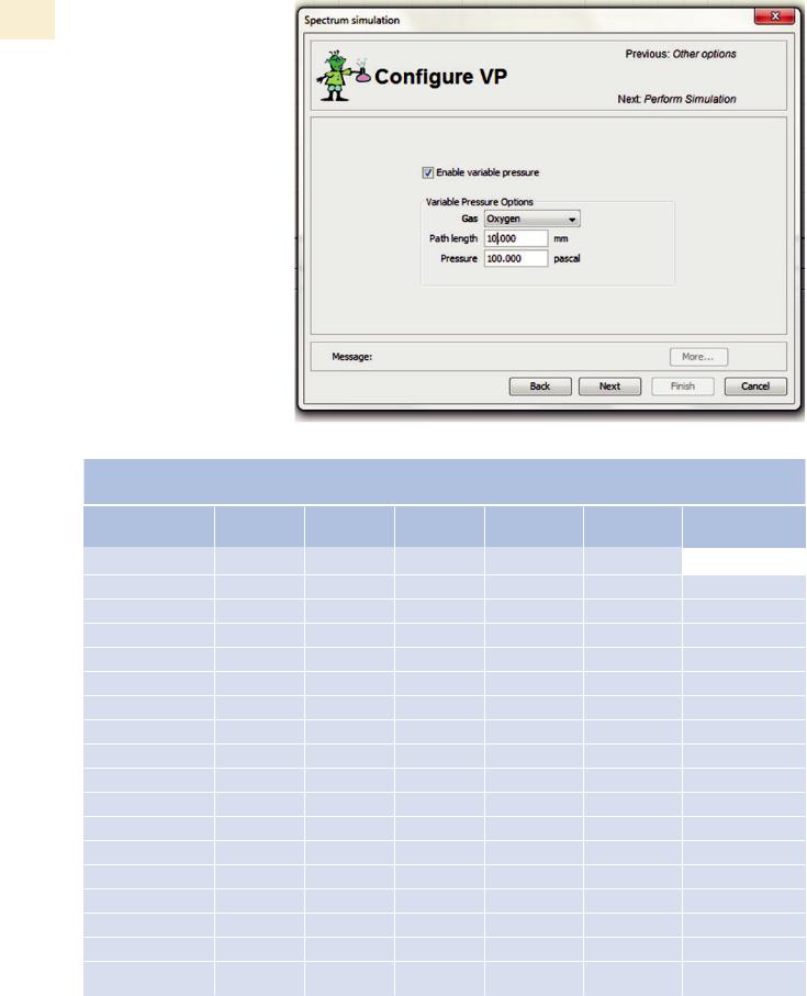
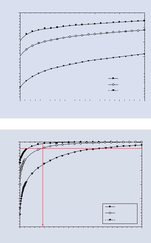
While Eq. (25.1) is useful to estimate the extent of the gas scattering on the spatial resolution of X-ray microanalysis under VPSEM conditions, it provides no information on the relative fractions of the spectrum that arise from the unscattered beam electrons (exactly equivalent to the high vacuum microanalysis footprint) and the skirt. The Monte Carlo simulation embedded in NIST DTSA-II enables explicit treatment of gas scattering to provide detailed information on the unscattered beam electrons and the distribution of electrons scattered into the skirt. The VPSEM menu of DTSA-II is shown in . Fig. 25.3 and allows selection of the gas path length, the gas pressure, and the gas species (He, N2, O2, H2O, or Ar). An example of a portion of the electron scattering information produced by the Monte Carlo simulation is listed in . Table 25.1 for a gas path length of 5 mm through 100 Pa of oxygen with a 20-keV beam energy; the full table extends to 1000 μm. This data set is plotted as the cumulative electron intensity as a function of radial distance out to 50 μm from the beam center in . Fig. 25.4. For these conditions the unscattered beam retains 0.70 of the beam intensity that enters the specimen chamber. The skirt out to a radius of 30 μm contains a cumulative intensity of 0.84 of the incident beam current. To capture 0.95 of the total current for a 5-mm gas path length in
. Fig. 25.2 Radial dimension of gas scattering skirt as a function of gas path length at various pressures for O2 and E0 = 20 keV
Development of beam “skirt”
Gas scattering skirt (oxygen; beam energy 20 keV)
|
100 |
|
|
|
|
|
|
|
|
|
1 Pa |
|
|
|
|
|
|
10 Pa |
|
|
|
80 |
|
|
100 Pa |
|
|
|
|
|
|
1000 Pa |
|
|
radius (micrometers) |
|
|
|
2500 Pa |
|
|
60 |
|
|
|
|
|
|
|
|
|
|
|
|
|
Skirt |
40 |
|
|
|
|
|
|
|
|
|
|
|
|
|
30 |
|
|
|
|
|
|
20 |
|
|
|
|
|
|
0 |
|
|
|
|
|
|
0 |
2 |
4 |
6 |
8 |
10 |
|
|
|
Gas path length (mm) |
|
|
|
444\ Chapter 25 · Attempting Electron-Excited X-Ray Microanalysis in the Variable Pressure Scanning Electron Microscope (VPSEM)
. Fig. 25.3 Selection of VPSEM 25 gas parameters in DTSA-II for
simulation
. Table 25.1 Portion of the electron scattering table for VPSEM simulation. Note the unscattered fraction of the 20 keV beam, 0.701
(100 Pa, 5-mm gas path length, oxygen). The full table extends to 1000 μm
Ring |
Inner radius, |
Outer radius, |
Ring area, |
Electron count |
Electron |
Cumulative, % |
|
μm |
μm |
μm2 |
|
fraction |
|
Undeflected |
– |
– |
– |
701 |
0.701 |
– |
|
|
|
|
|
|
|
1 |
0.0 |
2.5 |
19.6 |
755 |
0.755 |
75.5 |
2 |
2.5 |
5.0 |
58.9 |
23 |
0.023 |
77.8 |
3 |
5.0 |
7.5 |
98.2 |
11 |
0.011 |
78.9 |
4 |
7.5 |
10.0 |
137.4 |
10 |
0.010 |
79. 9 |
5 |
10.0 |
12.5 |
176.7 |
7 |
0.007 |
80.6 |
6 |
12.5 |
15.0 |
216.0 |
6 |
0.006 |
81.2 |
7 |
15.0 |
17.5 |
255.3 |
9 |
0.009 |
82.1 |
8 |
17.5 |
20.0 |
294.5 |
10 |
0.010 |
83.1 |
9 |
20.0 |
22.5 |
333.8 |
4 |
0.004 |
83.5 |
10 |
22.5 |
25.0 |
373.1 |
3i |
0.003 |
83.8 |
11 |
25.0 |
27.5 |
412.3 |
6 |
0.006 |
84.4 |
12 |
27.5 |
30.0 |
451.6 |
4 |
0.004 |
84.8 |
13 |
30.0 |
32.5 |
490.9 |
6 |
0.006 |
85.4 |
14 |
32.5 |
35.0 |
530.1 |
2 |
0.002 |
85.6 |
15 |
35.0 |
37.5 |
569.4 |
2 |
0.002 |
85.8 |
16 |
37.5 |
40.0 |
608.7 |
3 |
0.003 |
86.1 |
17 |
40.0 |
42.5 |
648.0 |
4 |
0.004 |
86.5 |
25.1 · Gas Scattering Effects in the VPSEM
. Fig. 25.4 DTSA-II Monte Carlo calculation of gas scattering in a VPSEM: E0 = 20 keV; oxygen; 100 Pa; 3-, 5-, and 10-mm gas path lengths (GPL) to a radial distance of 50 μm
Cumulative electron intensity
445 |
|
25 |
|
|
|
VPSEM 100 Pa O2
1.0
0.9
0.8 
0.7 

0.6 |
|
|
|
|
|
|
|
|
|
|
|
|
|
|
|
|
|
|
|
|
|
|
|
|
|
|
|
|
|
|
|
|
|
|
|
|
|
|
|
|
|
|
|
|
|
|
|
|
|
|
|
|
|
|
|
|
|
|
|
|
|
|
|
3 mm GPL |
|
|
|
0.5 |
|
|
|
|
|
|
|
|
|
|
|
|
5 mm GPL |
|
|
|
|
|
|
|
|
|
|
|
|
|
|
|
10 mm GPL |
|
|
|
|
|
|
|
|
|
|
|
|
|
|
|
|
|
|
|
|
|
0.4 |
|
|
|
|
|
|
|
|
|
|
|
|
|
|
|
|
|
|
|
|
|
|
|
|
|
|
|
|
|
|
|
|
|
0 |
10 |
20 |
30 |
40 |
50 |
|||||||||||
Radial distance from beam center (micrometers)
. Fig. 25.5 DTSA-II Monte Carlo calculation of gas scattering in a VPSEM: E0 = 20 keV; oxygen; 100 Pa; 3-, 5-, and 10-mm gas path lengths to a radial distance of 1000 μm
|
|
VPSEM 100 Pa O2 |
|
1.0 |
|
|
0.9 |
|
electron intensity |
0.8 |
|
0.7 |
|
|
Cumulative |
0.6 |
|
|
3 mm GPL |
|
|
|
|
|
0.5 |
5 mm GPL |
|
|
10 mm GPL |
|
0.4 |
|
0 |
200 |
400 |
600 |
800 |
1000 |
|
Radial distance from beam center (micrometers) |
|
|||
100 Pa of oxygen requires a radial distance of approximately 190 μm, as shown in . Fig. 25.5, which plots the skirt distribution out to 1000 μm (1 mm). The strong effect of the gas path length on the skirt radius, which follows a 3/2 exponent in the scattering Eq. 25.1, can be seen in . Fig. 25.5 in the plots for 3 mm, 5 mm, and 10 mm gas path lengths.
The extent of the degradation of the measured EDS spectrum by gas scattering is illustrated in the experiment shown in . Fig. 25.6. The incident beam is placed at the center of a polished cross section of a 40 wt % Cu – 60 wt % Au alloy wire 500 μm in diameter surrounded by a 2.5-cm-diameter Al disk. For a beam energy of 20 keV and a gas path length of