

- •Preface
- •Imaging Microscopic Features
- •Measuring the Crystal Structure
- •References
- •Contents
- •1.4 Simulating the Effects of Elastic Scattering: Monte Carlo Calculations
- •What Are the Main Features of the Beam Electron Interaction Volume?
- •How Does the Interaction Volume Change with Composition?
- •How Does the Interaction Volume Change with Incident Beam Energy?
- •How Does the Interaction Volume Change with Specimen Tilt?
- •1.5 A Range Equation To Estimate the Size of the Interaction Volume
- •References
- •2: Backscattered Electrons
- •2.1 Origin
- •2.2.1 BSE Response to Specimen Composition (η vs. Atomic Number, Z)
- •SEM Image Contrast with BSE: “Atomic Number Contrast”
- •SEM Image Contrast: “BSE Topographic Contrast—Number Effects”
- •2.2.3 Angular Distribution of Backscattering
- •Beam Incident at an Acute Angle to the Specimen Surface (Specimen Tilt > 0°)
- •SEM Image Contrast: “BSE Topographic Contrast—Trajectory Effects”
- •2.2.4 Spatial Distribution of Backscattering
- •Depth Distribution of Backscattering
- •Radial Distribution of Backscattered Electrons
- •2.3 Summary
- •References
- •3: Secondary Electrons
- •3.1 Origin
- •3.2 Energy Distribution
- •3.3 Escape Depth of Secondary Electrons
- •3.8 Spatial Characteristics of Secondary Electrons
- •References
- •4: X-Rays
- •4.1 Overview
- •4.2 Characteristic X-Rays
- •4.2.1 Origin
- •4.2.2 Fluorescence Yield
- •4.2.3 X-Ray Families
- •4.2.4 X-Ray Nomenclature
- •4.2.6 Characteristic X-Ray Intensity
- •Isolated Atoms
- •X-Ray Production in Thin Foils
- •X-Ray Intensity Emitted from Thick, Solid Specimens
- •4.3 X-Ray Continuum (bremsstrahlung)
- •4.3.1 X-Ray Continuum Intensity
- •4.3.3 Range of X-ray Production
- •4.4 X-Ray Absorption
- •4.5 X-Ray Fluorescence
- •References
- •5.1 Electron Beam Parameters
- •5.2 Electron Optical Parameters
- •5.2.1 Beam Energy
- •Landing Energy
- •5.2.2 Beam Diameter
- •5.2.3 Beam Current
- •5.2.4 Beam Current Density
- •5.2.5 Beam Convergence Angle, α
- •5.2.6 Beam Solid Angle
- •5.2.7 Electron Optical Brightness, β
- •Brightness Equation
- •5.2.8 Focus
- •Astigmatism
- •5.3 SEM Imaging Modes
- •5.3.1 High Depth-of-Field Mode
- •5.3.2 High-Current Mode
- •5.3.3 Resolution Mode
- •5.3.4 Low-Voltage Mode
- •5.4 Electron Detectors
- •5.4.1 Important Properties of BSE and SE for Detector Design and Operation
- •Abundance
- •Angular Distribution
- •Kinetic Energy Response
- •5.4.2 Detector Characteristics
- •Angular Measures for Electron Detectors
- •Elevation (Take-Off) Angle, ψ, and Azimuthal Angle, ζ
- •Solid Angle, Ω
- •Energy Response
- •Bandwidth
- •5.4.3 Common Types of Electron Detectors
- •Backscattered Electrons
- •Passive Detectors
- •Scintillation Detectors
- •Semiconductor BSE Detectors
- •5.4.4 Secondary Electron Detectors
- •Everhart–Thornley Detector
- •Through-the-Lens (TTL) Electron Detectors
- •TTL SE Detector
- •TTL BSE Detector
- •Measuring the DQE: BSE Semiconductor Detector
- •References
- •6: Image Formation
- •6.1 Image Construction by Scanning Action
- •6.2 Magnification
- •6.3 Making Dimensional Measurements With the SEM: How Big Is That Feature?
- •Using a Calibrated Structure in ImageJ-Fiji
- •6.4 Image Defects
- •6.4.1 Projection Distortion (Foreshortening)
- •6.4.2 Image Defocusing (Blurring)
- •6.5 Making Measurements on Surfaces With Arbitrary Topography: Stereomicroscopy
- •6.5.1 Qualitative Stereomicroscopy
- •Fixed beam, Specimen Position Altered
- •Fixed Specimen, Beam Incidence Angle Changed
- •6.5.2 Quantitative Stereomicroscopy
- •Measuring a Simple Vertical Displacement
- •References
- •7: SEM Image Interpretation
- •7.1 Information in SEM Images
- •7.2.2 Calculating Atomic Number Contrast
- •Establishing a Robust Light-Optical Analogy
- •Getting It Wrong: Breaking the Light-Optical Analogy of the Everhart–Thornley (Positive Bias) Detector
- •Deconstructing the SEM/E–T Image of Topography
- •SUM Mode (A + B)
- •DIFFERENCE Mode (A−B)
- •References
- •References
- •9: Image Defects
- •9.1 Charging
- •9.1.1 What Is Specimen Charging?
- •9.1.3 Techniques to Control Charging Artifacts (High Vacuum Instruments)
- •Observing Uncoated Specimens
- •Coating an Insulating Specimen for Charge Dissipation
- •Choosing the Coating for Imaging Morphology
- •9.2 Radiation Damage
- •9.3 Contamination
- •References
- •10: High Resolution Imaging
- •10.2 Instrumentation Considerations
- •10.4.1 SE Range Effects Produce Bright Edges (Isolated Edges)
- •10.4.4 Too Much of a Good Thing: The Bright Edge Effect Hinders Locating the True Position of an Edge for Critical Dimension Metrology
- •10.5.1 Beam Energy Strategies
- •Low Beam Energy Strategy
- •High Beam Energy Strategy
- •Making More SE1: Apply a Thin High-δ Metal Coating
- •Making Fewer BSEs, SE2, and SE3 by Eliminating Bulk Scattering From the Substrate
- •10.6 Factors That Hinder Achieving High Resolution
- •10.6.2 Pathological Specimen Behavior
- •Contamination
- •Instabilities
- •References
- •11: Low Beam Energy SEM
- •11.3 Selecting the Beam Energy to Control the Spatial Sampling of Imaging Signals
- •11.3.1 Low Beam Energy for High Lateral Resolution SEM
- •11.3.2 Low Beam Energy for High Depth Resolution SEM
- •11.3.3 Extremely Low Beam Energy Imaging
- •References
- •12.1.1 Stable Electron Source Operation
- •12.1.2 Maintaining Beam Integrity
- •12.1.4 Minimizing Contamination
- •12.3.1 Control of Specimen Charging
- •12.5 VPSEM Image Resolution
- •References
- •13: ImageJ and Fiji
- •13.1 The ImageJ Universe
- •13.2 Fiji
- •13.3 Plugins
- •13.4 Where to Learn More
- •References
- •14: SEM Imaging Checklist
- •14.1.1 Conducting or Semiconducting Specimens
- •14.1.2 Insulating Specimens
- •14.2 Electron Signals Available
- •14.2.1 Beam Electron Range
- •14.2.2 Backscattered Electrons
- •14.2.3 Secondary Electrons
- •14.3 Selecting the Electron Detector
- •14.3.2 Backscattered Electron Detectors
- •14.3.3 “Through-the-Lens” Detectors
- •14.4 Selecting the Beam Energy for SEM Imaging
- •14.4.4 High Resolution SEM Imaging
- •Strategy 1
- •Strategy 2
- •14.5 Selecting the Beam Current
- •14.5.1 High Resolution Imaging
- •14.5.2 Low Contrast Features Require High Beam Current and/or Long Frame Time to Establish Visibility
- •14.6 Image Presentation
- •14.6.1 “Live” Display Adjustments
- •14.6.2 Post-Collection Processing
- •14.7 Image Interpretation
- •14.7.1 Observer’s Point of View
- •14.7.3 Contrast Encoding
- •14.8.1 VPSEM Advantages
- •14.8.2 VPSEM Disadvantages
- •15: SEM Case Studies
- •15.1 Case Study: How High Is That Feature Relative to Another?
- •15.2 Revealing Shallow Surface Relief
- •16.1.2 Minor Artifacts: The Si-Escape Peak
- •16.1.3 Minor Artifacts: Coincidence Peaks
- •16.1.4 Minor Artifacts: Si Absorption Edge and Si Internal Fluorescence Peak
- •16.2 “Best Practices” for Electron-Excited EDS Operation
- •16.2.1 Operation of the EDS System
- •Choosing the EDS Time Constant (Resolution and Throughput)
- •Choosing the Solid Angle of the EDS
- •Selecting a Beam Current for an Acceptable Level of System Dead-Time
- •16.3.1 Detector Geometry
- •16.3.2 Process Time
- •16.3.3 Optimal Working Distance
- •16.3.4 Detector Orientation
- •16.3.5 Count Rate Linearity
- •16.3.6 Energy Calibration Linearity
- •16.3.7 Other Items
- •16.3.8 Setting Up a Quality Control Program
- •Using the QC Tools Within DTSA-II
- •Creating a QC Project
- •Linearity of Output Count Rate with Live-Time Dose
- •Resolution and Peak Position Stability with Count Rate
- •Solid Angle for Low X-ray Flux
- •Maximizing Throughput at Moderate Resolution
- •References
- •17: DTSA-II EDS Software
- •17.1 Getting Started With NIST DTSA-II
- •17.1.1 Motivation
- •17.1.2 Platform
- •17.1.3 Overview
- •17.1.4 Design
- •Simulation
- •Quantification
- •Experiment Design
- •Modeled Detectors (. Fig. 17.1)
- •Window Type (. Fig. 17.2)
- •The Optimal Working Distance (. Figs. 17.3 and 17.4)
- •Elevation Angle
- •Sample-to-Detector Distance
- •Detector Area
- •Crystal Thickness
- •Number of Channels, Energy Scale, and Zero Offset
- •Resolution at Mn Kα (Approximate)
- •Azimuthal Angle
- •Gold Layer, Aluminum Layer, Nickel Layer
- •Dead Layer
- •Zero Strobe Discriminator (. Figs. 17.7 and 17.8)
- •Material Editor Dialog (. Figs. 17.9, 17.10, 17.11, 17.12, 17.13, and 17.14)
- •17.2.1 Introduction
- •17.2.2 Monte Carlo Simulation
- •17.2.4 Optional Tables
- •References
- •18: Qualitative Elemental Analysis by Energy Dispersive X-Ray Spectrometry
- •18.1 Quality Assurance Issues for Qualitative Analysis: EDS Calibration
- •18.2 Principles of Qualitative EDS Analysis
- •Exciting Characteristic X-Rays
- •Fluorescence Yield
- •X-ray Absorption
- •Si Escape Peak
- •Coincidence Peaks
- •18.3 Performing Manual Qualitative Analysis
- •Beam Energy
- •Choosing the EDS Resolution (Detector Time Constant)
- •Obtaining Adequate Counts
- •18.4.1 Employ the Available Software Tools
- •18.4.3 Lower Photon Energy Region
- •18.4.5 Checking Your Work
- •18.5 A Worked Example of Manual Peak Identification
- •References
- •19.1 What Is a k-ratio?
- •19.3 Sets of k-ratios
- •19.5 The Analytical Total
- •19.6 Normalization
- •19.7.1 Oxygen by Assumed Stoichiometry
- •19.7.3 Element by Difference
- •19.8 Ways of Reporting Composition
- •19.8.1 Mass Fraction
- •19.8.2 Atomic Fraction
- •19.8.3 Stoichiometry
- •19.8.4 Oxide Fractions
- •Example Calculations
- •19.9 The Accuracy of Quantitative Electron-Excited X-ray Microanalysis
- •19.9.1 Standards-Based k-ratio Protocol
- •19.9.2 “Standardless Analysis”
- •19.10 Appendix
- •19.10.1 The Need for Matrix Corrections To Achieve Quantitative Analysis
- •19.10.2 The Physical Origin of Matrix Effects
- •19.10.3 ZAF Factors in Microanalysis
- •X-ray Generation With Depth, φ(ρz)
- •X-ray Absorption Effect, A
- •X-ray Fluorescence, F
- •References
- •20.2 Instrumentation Requirements
- •20.2.1 Choosing the EDS Parameters
- •EDS Spectrum Channel Energy Width and Spectrum Energy Span
- •EDS Time Constant (Resolution and Throughput)
- •EDS Calibration
- •EDS Solid Angle
- •20.2.2 Choosing the Beam Energy, E0
- •20.2.3 Measuring the Beam Current
- •20.2.4 Choosing the Beam Current
- •Optimizing Analysis Strategy
- •20.3.4 Ba-Ti Interference in BaTiSi3O9
- •20.4 The Need for an Iterative Qualitative and Quantitative Analysis Strategy
- •20.4.2 Analysis of a Stainless Steel
- •20.5 Is the Specimen Homogeneous?
- •20.6 Beam-Sensitive Specimens
- •20.6.1 Alkali Element Migration
- •20.6.2 Materials Subject to Mass Loss During Electron Bombardment—the Marshall-Hall Method
- •Thin Section Analysis
- •Bulk Biological and Organic Specimens
- •References
- •21: Trace Analysis by SEM/EDS
- •21.1 Limits of Detection for SEM/EDS Microanalysis
- •21.2.1 Estimating CDL from a Trace or Minor Constituent from Measuring a Known Standard
- •21.2.2 Estimating CDL After Determination of a Minor or Trace Constituent with Severe Peak Interference from a Major Constituent
- •21.3 Measurements of Trace Constituents by Electron-Excited Energy Dispersive X-ray Spectrometry
- •The Inevitable Physics of Remote Excitation Within the Specimen: Secondary Fluorescence Beyond the Electron Interaction Volume
- •Simulation of Long-Range Secondary X-ray Fluorescence
- •NIST DTSA II Simulation: Vertical Interface Between Two Regions of Different Composition in a Flat Bulk Target
- •NIST DTSA II Simulation: Cubic Particle Embedded in a Bulk Matrix
- •21.5 Summary
- •References
- •22.1.2 Low Beam Energy Analysis Range
- •22.2 Advantage of Low Beam Energy X-Ray Microanalysis
- •22.2.1 Improved Spatial Resolution
- •22.3 Challenges and Limitations of Low Beam Energy X-Ray Microanalysis
- •22.3.1 Reduced Access to Elements
- •22.3.3 At Low Beam Energy, Almost Everything Is Found To Be Layered
- •Analysis of Surface Contamination
- •References
- •23: Analysis of Specimens with Special Geometry: Irregular Bulk Objects and Particles
- •23.2.1 No Chemical Etching
- •23.3 Consequences of Attempting Analysis of Bulk Materials With Rough Surfaces
- •23.4.1 The Raw Analytical Total
- •23.4.2 The Shape of the EDS Spectrum
- •23.5 Best Practices for Analysis of Rough Bulk Samples
- •23.6 Particle Analysis
- •Particle Sample Preparation: Bulk Substrate
- •The Importance of Beam Placement
- •Overscanning
- •“Particle Mass Effect”
- •“Particle Absorption Effect”
- •The Analytical Total Reveals the Impact of Particle Effects
- •Does Overscanning Help?
- •23.6.6 Peak-to-Background (P/B) Method
- •Specimen Geometry Severely Affects the k-ratio, but Not the P/B
- •Using the P/B Correspondence
- •23.7 Summary
- •References
- •24: Compositional Mapping
- •24.2 X-Ray Spectrum Imaging
- •24.2.1 Utilizing XSI Datacubes
- •24.2.2 Derived Spectra
- •SUM Spectrum
- •MAXIMUM PIXEL Spectrum
- •24.3 Quantitative Compositional Mapping
- •24.4 Strategy for XSI Elemental Mapping Data Collection
- •24.4.1 Choosing the EDS Dead-Time
- •24.4.2 Choosing the Pixel Density
- •24.4.3 Choosing the Pixel Dwell Time
- •“Flash Mapping”
- •High Count Mapping
- •References
- •25.1 Gas Scattering Effects in the VPSEM
- •25.1.1 Why Doesn’t the EDS Collimator Exclude the Remote Skirt X-Rays?
- •25.2 What Can Be Done To Minimize gas Scattering in VPSEM?
- •25.2.2 Favorable Sample Characteristics
- •Particle Analysis
- •25.2.3 Unfavorable Sample Characteristics
- •References
- •26.1 Instrumentation
- •26.1.2 EDS Detector
- •26.1.3 Probe Current Measurement Device
- •Direct Measurement: Using a Faraday Cup and Picoammeter
- •A Faraday Cup
- •Electrically Isolated Stage
- •Indirect Measurement: Using a Calibration Spectrum
- •26.1.4 Conductive Coating
- •26.2 Sample Preparation
- •26.2.1 Standard Materials
- •26.2.2 Peak Reference Materials
- •26.3 Initial Set-Up
- •26.3.1 Calibrating the EDS Detector
- •Selecting a Pulse Process Time Constant
- •Energy Calibration
- •Quality Control
- •Sample Orientation
- •Detector Position
- •Probe Current
- •26.4 Collecting Data
- •26.4.1 Exploratory Spectrum
- •26.4.2 Experiment Optimization
- •26.4.3 Selecting Standards
- •26.4.4 Reference Spectra
- •26.4.5 Collecting Standards
- •26.4.6 Collecting Peak-Fitting References
- •26.5 Data Analysis
- •26.5.2 Quantification
- •26.6 Quality Check
- •Reference
- •27.2 Case Study: Aluminum Wire Failures in Residential Wiring
- •References
- •28: Cathodoluminescence
- •28.1 Origin
- •28.2 Measuring Cathodoluminescence
- •28.3 Applications of CL
- •28.3.1 Geology
- •Carbonado Diamond
- •Ancient Impact Zircons
- •28.3.2 Materials Science
- •Semiconductors
- •Lead-Acid Battery Plate Reactions
- •28.3.3 Organic Compounds
- •References
- •29.1.1 Single Crystals
- •29.1.2 Polycrystalline Materials
- •29.1.3 Conditions for Detecting Electron Channeling Contrast
- •Specimen Preparation
- •Instrument Conditions
- •29.2.1 Origin of EBSD Patterns
- •29.2.2 Cameras for EBSD Pattern Detection
- •29.2.3 EBSD Spatial Resolution
- •29.2.5 Steps in Typical EBSD Measurements
- •Sample Preparation for EBSD
- •Align Sample in the SEM
- •Check for EBSD Patterns
- •Adjust SEM and Select EBSD Map Parameters
- •Run the Automated Map
- •29.2.6 Display of the Acquired Data
- •29.2.7 Other Map Components
- •29.2.10 Application Example
- •Application of EBSD To Understand Meteorite Formation
- •29.2.11 Summary
- •Specimen Considerations
- •EBSD Detector
- •Selection of Candidate Crystallographic Phases
- •Microscope Operating Conditions and Pattern Optimization
- •Selection of EBSD Acquisition Parameters
- •Collect the Orientation Map
- •References
- •30.1 Introduction
- •30.2 Ion–Solid Interactions
- •30.3 Focused Ion Beam Systems
- •30.5 Preparation of Samples for SEM
- •30.5.1 Cross-Section Preparation
- •30.5.2 FIB Sample Preparation for 3D Techniques and Imaging
- •30.6 Summary
- •References
- •31: Ion Beam Microscopy
- •31.1 What Is So Useful About Ions?
- •31.2 Generating Ion Beams
- •31.3 Signal Generation in the HIM
- •31.5 Patterning with Ion Beams
- •31.7 Chemical Microanalysis with Ion Beams
- •References
- •Appendix
- •A Database of Electron–Solid Interactions
- •A Database of Electron–Solid Interactions
- •Introduction
- •Backscattered Electrons
- •Secondary Yields
- •Stopping Powers
- •X-ray Ionization Cross Sections
- •Conclusions
- •References
- •Index
- •Reference List
- •Index

18.5 · A Worked Example of Manual Peak Identification
18.4.3\ Lower Photon Energy Region
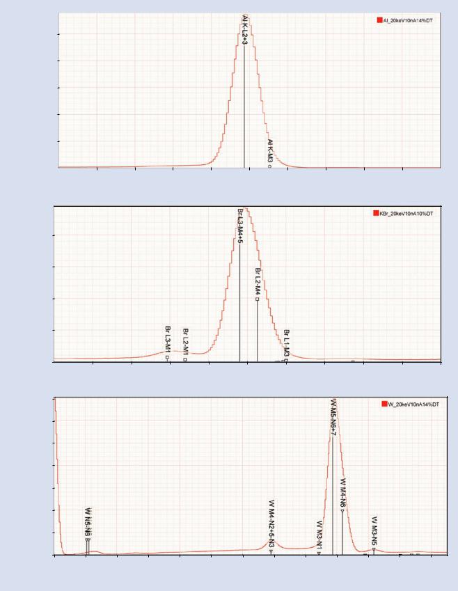
As major spectral peaks located at lower photon energy (<4 keV) are considered, the energy separation diminishes and the relative peak heights decrease for the members of each X-ray family. EDS is no longer able to resolve these peaks, leading to a situation where only one peak is available for identification for K-family X-rays below 2 keV in energy. The K-L3 peak appears symmetric since the K-M3 peak has low relative intensity, as shown for Al K-L3 in . Fig. 18.13a. For L- and M- family X-rays in the low photon energy range, the composite peak appears asymmetric. As shown for Br in . Fig. 18.13b, the major peaks L3-M5(Lα) and L2-M4(Lβ) occur with a ratio of approximately 2:1 and the low abundance but separated L3- M1 (Ll) and L2-M1 (Lη) can also aid in the identification providing the spectrum contains adequate counts. Similarly, the
M5-N6,7(Mα) and M4-N6(Mβ) peaks occur with a ratio of 1/0.6 and the well separated minor family members W M5,4-N3,2
(Mζ) and W M3-N5 (Mγ) can be detected in a high count spectrum, as shown for W in . Fig. 18.13c.
18.4.4\ Identifying the Peaks: Minor
and Trace Constituents
After all major peaks and their associated minor family members and artifact peaks have been located and identified with high confidence as belonging to particular elements, the analyst can proceed to identify any remaining peaks which are now likely to be associated with minor and trace level constituents. Achieving the same degree of high confidence in the identification of lower concentration constituents is more difficult since the lower concentrations reduce all X-ray intensities so that minor family members are more difficult to detect. The situation is likely to require accumulating additional X-ray counts to improve the detectability of minor X-ray family members and increase the confidence of the assignment of elemental identification. In general, establishing the presence of a constituent at trace level is a significant challenge that requires not only collecting a high count spectrum that satisfies the limit of detection criterion but also scrupulous attention to identifying all possible minor family members and artifacts from the X-ray families of the major and minor constituents.
18.4.5\ Checking Your Work
The only way to be confident that the qualitative analysis is correct to quantify the spectrum and examine the residual spectrum. When every element has been correctly identified and quantified, the analytical total should be approximately unity and there should be no obvious structure in the residual spectrum that cannot be explained through chemistry or minor chemical peak shifts. This iterative qualitative – quantitative analysis scheme to discover minor and trace elements hidden under the high intensity peaks of major constituents will covered in 7 Chapter 19.
281 |
|
18 |
|
|
|
18.5\ A Worked Example of Manual Peak
Identification
Alloy IN100 is a complex mixture of transition and heavy elements that provides several challenges to manual peak identification:
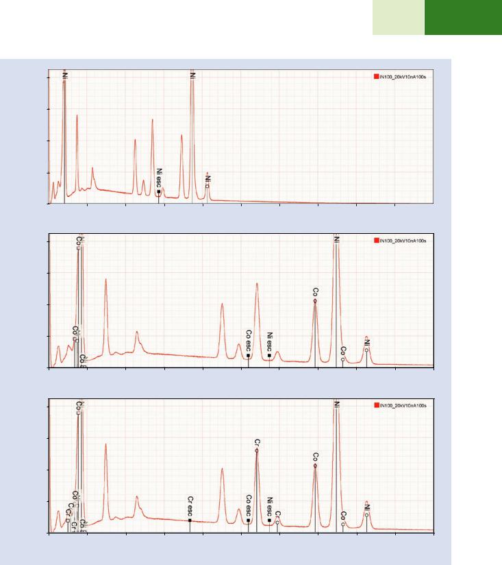
1. . Figure 18.14a shows the spectrum from 0 to 20 keV excited with E0 = 20 keV. Using the KLM marker tools in DTSA II, starting at high photon energy and working downward, the first high peak encountered shows a good match to Ni K-L3 and the corresponding Ni K-M3 is also found at the correct ratio, as well as the Ni L-family at low photon energy. The position of the Ni K-L3 escape peak is marked. Inspection for possible coincidence peaks does not reveal a significant population due to the low dead-time (8 %) used to accumulate the spectrum and the large number of peaks over which the input count rate is partitioned so that even the most intense peak has a relatively low count rate and does not produce significant coincidence.
\2.\ Working down in energy (. Fig. 18.14b), the next peak is seen to correspond to Co K-L3, but the Co K-M3 suffers interference from Ni K-L3 and only appears as an asymmetric deviation on the high energy side. Likewise, the Co L-family is unresolved from the Ni L-family.
\3.\ The next set of peaks match Cr, as shown in . Fig. 18.14c.
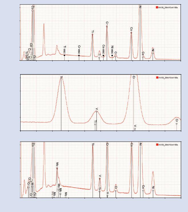
4.Continuing, . Fig. 18.14d shows a match for the peaks of
Ti, but the apparent ratio of Ti K-L3/Ti K-M3 is approximately 5:1, whereas the true ratio is about 10:1, which suggests that another element must be present. Expansion of this region in . Fig. 18.14e reveals that V is likely to be present but with severe interference between
V K-L3 and Ti K-M3. While the anomalous peak ratio observed for TiK-L3/TiK-M3 is a strong clue that another element must be present, this example shows one of the limitations of manual peak identification, namely, that peaks representing minor and trace constituents can be lost under the higher intensity peaks of higher concentration constituents as the concentration ratio becomes large. Detecting such interferences of constituents with large concentration ratios requires the careful peak- fitting procedure that is embedded in the quantitative analysis procedures described in module 19.
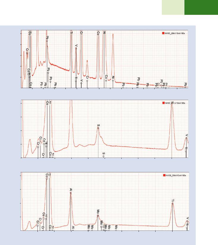
5.In . Fig. 18.14f, the next peak group best matches the Mo L-family. This photon energy range involves possible interferences from the S K-family, the Mo L-family, and the Pb M-family. The possibility of identifying the peak group as the Pb M-family which occurs this energy range, can be rejected because of the absence of the Pb L-family, as shown in . Fig. 18.14g. The possible presence of the S K-family (. Fig. 18.14h) is much more difficult to exclude because S cannot be effectively measured by an alternate X-ray family such as the S L-family due to the low fluorescence yield. While the
shape of the peak cluster does not match S K-L3 and S K-M3, the presence of S can only be confidently
\282 Chapter 18 · Qualitative Elemental Analysis by Energy Dispersive X-Ray Spectrometry
a
Counts
10 00 000 |
|
|
|
|
|
|
|
|
|
|
|
|
|
800 000 |
|
|
|
|
|
|
|
|
Al |
|
|
|
|
|
|
|
|
|
|
|
|
|
|
|
|
|
|
|
|
|
|
|
|
|
|
|
E0 = 20 keV |
|
|
|
|
600 000 |
|
|
|
|
|
|
|
|
|
|
|
|
|
400 000 |
|
|
|
|
|
|
|
|
|
|
|
|
|
200 000 |
|
|
|
|
|
|
|
|
|
|
|
|
|
0 |
|
|
|
|
|
|
|
|
|
|
|
|
|
|
|
|
|
|
|
|
|
|
|
|
|
|
|
1.00 |
1.10 |
1.20 |
1.30 |
1.40 |
1.50 |
1.60 |
1.70 |
1.80 |
1.90 |
2.00 |
|||
Photon energy (keV)
|
b |
200 000 |
|
|
|
||
|
|
|
|
|
|
150 000 |
|
|
Counts |
100 000 |
|
|
|
|
|
|
|
50 000 |
|
|
|
0 |
|
|
|
|
|
|
|
1.00 |
|
|
c |
|
|
|
|
350 000 |
|
|
|
|
|
|
|
300 000 |
|
|
|
250 000 |
|
18 |
Counts |
200 000 |
|
|
150 000 |
|
|
|
|
|
|
|
|
100 000 |
|
|
|
50 000 |
|
|
|
0 |
|
|
|
|
|
|
|
0.0 |
|
KBr
E0 = 20 keV
1.10 |
1.20 |
1.30 |
1.40 |
1.50 |
1.60 |
1.70 |
1.80 |
1.90 |
2.00 |
|
|
|
|
Photon energy (keV) |
|
|
|
|
|
W
E0 = 20 keV
0.2 |
0.4 |
0.6 |
0.8 |
1.0 |
1.2 |
1.4 |
1.6 |
1.8 |
2.0 |
2.2 |
2.4 |
|
|
|
|
|
Photon energy (keV) |
|
|
|
|
|
|
. Fig. 18.13 a EDS spectrum of Al at E0 = 20 keV; note symmetry of Al K-family peaks. b EDS spectrum of KBr at E0 = 20 keV; note asymmetry of Br L-family peaks. c EDS spectrum of W at E0 = 20 keV; note asymmetry of W M-family peaks
18.5 ·
a
Counts
283 |
18 |
A Worked Example of Manual Peak Identification
40 000 |
|
|
|
IN100 |
|
30 000 |
E0 = 20 keV |
|
8% deadtime |
||
|
||
20 000 |
|
|
10 000 |
|
|
0 |
|
|
|
0 |
2 |
4 |
6 |
8 |
10 |
12 |
14 |
16 |
18 |
20 |
|
|
|
|
|
Photon energy (keV) |
|
|
|
|
|
b
Counts
c
Counts
40 000
30 000
20 000
10 000
0
0.0
40 000
30 000
20 000
10 000
0
0.0
1.0 |
2.0 |
3.0 |
4.0 |
5.0 |
6.0 |
7.0 |
8.0 |
9.0 |
10.0 |
Photon energy (keV)
IN100
E0 = 20 keV 8% deadtime
1.0 |
2.0 |
3.0 |
4.0 |
5.0 |
6.0 |
7.0 |
8.0 |
9.0 |
10.0 |
|
|
|
|
Photon energy (keV) |
|
|
|
|
|
. Fig. 18.14 a Alloy IN100 recorded with E0 = 20 keV and at 8 % dead-time showing identification of Ni. b Identification of Co. c Identification of Cr. d Identification of Ti. e Identification of V. f Identification
of Mo. g Rejection of Pb. h Possible presence of S. i Identification of Al. j Rejection of Br. k Identification of C. l Identification of Si
\284 Chapter 18 · Qualitative Elemental Analysis by Energy Dispersive X-Ray Spectrometry
|
d |
40 000 |
|
|
|
|
30 000 |
|
|
|
Counts |
20 000 |
|
|
|
|
10 000 |
|
|
|
|
0 |
|
|
|
|
0.0 |
||
|
e |
20 000 |
|
|
|
|
|
||
|
|
15 000 |
|
|
|
Counts |
10 000 |
|
|
|
|
5 000 |
|
|
|
f |
04.0 |
||
|
20 000 |
|
||
|
|
|||
|
|
|
||
|
|
15 000 |
|
|
|
Counts |
10 000 |
|
|
|
|
|
||
|
|
5 000 |
|
|
18 |
|
|||
|
|
|
|
|
|
|
0 |
|
|
|
|
|
||
|
|
|
||
|
|
|
0.0 |
|
1.0 |
2.0 |
3.0 |
4.0 |
5.0 |
6.0 |
7.0 |
8.0 |
9.0 |
10.0 |
Photon energy (keV)
IN100
E0 = 20 keV 8% deadtime
4.2 |
4.4 |
4.6 |
4.8 |
5.0 |
5.2 |
5.4 |
5.6 |
5.8 |
6.0 |
|
|
|
|
Photon energy (keV) |
|
|
|
|
|
1.0 |
2.0 |
3.0 |
4.0 |
5.0 |
6.0 |
7.0 |
8.0 |
9.0 |
10.0 |
Photon energy (keV)
. Fig. 18.14 (continued)
285 |
18 |
18.5 · A Worked Example of Manual Peak Identification
g
Counts
h
Counts
i
Counts
10 000 |
|
|
|
|
|
|
|
|
|
|
|
|
|
|
|
|
|
|
|
|
|
|
|
|
|
|
|
|
|
|
|
IN100 |
|
|
|
|
|
|
|
8 000 |
|
|
|
|
|
|
|
|
|
|
|
E0 = 20 keV |
|
|
|
|
|
|
|
|
|
|
|
|
|
|
|
|
|
|
8% deadtime |
|
|
|
|
|
|
||
|
|
|
|
|
|
|
|
|
|
|
|
|
|
|
|
|
|
||
6 000 |
|
|
|
|
|
|
|
|
|
|
|
|
|
|
|
|
|
|
|
4 000 |
|
|
|
|
|
|
|
|
|
|
|
|
|
|
|
|
|
|
|
2 000 |
|
|
|
|
|
|
|
|
|
|
|
|
|
|
|
|
|
|
|
0 |
|
|
|
|
|
|
|
|
|
|
|
|
|
|
|
|
|
|
|
0.0 |
1.0 |
2.0 |
3.0 |
4.0 |
5.0 |
6.0 |
7.0 |
8.0 |
9.0 |
10.0 |
11.0 |
12.0 |
13.0 |
14.0 |
15.0 |
||||
|
|
|
|
|
|
|
|
|
Photon energy (keV) |
|
|
|
|
|
|
|
|
|
|
20 000 |
|
|
|
|
|
|
|
|
|
|
|
|
|
|
|
|
|
|
|
|
|
|
|
|
|
|
|
|
|
|
|
|
|
|
|
|
|
|
|
15 000 |
|
|
|
|
|
|
|
|
|
|
|
|
|
|
|
|
|
|
|
10 000 |
|
|
|
|
|
|
|
|
|
|
|
|
|
|
|
|
|
|
|
5 000 |
|
|
|
|
|
|
|
|
|
|
|
|
|
|
|
|
|
|
|
0 |
|
|
|
|
|
|
|
|
|
|
|
|
|
|
|
|
|
|
|
|
|
|
|
|
|
|
|
|
|
|
|
|
|
|
|
|
|
||
0.0 |
|
0.5 |
1.0 |
|
1.5 |
2.0 |
|
2.5 |
3.0 |
|
3.5 |
4.0 |
|
4.5 |
5.0 |
||||
|
|
|
|
|
|
|
|
|
Photon energy (keV) |
|
|
|
|
|
|
|
|
||
40 000 |
|
|
|
|
|
|
|
|
|
|
|
|
|
|
|
|
|
|
|
|
|
|
|
|
|
|
|
|
|
|
|
|
|
|
|
|
|
|
|
|
|
|
|
|
|
|
|
|
|
|
|
IN100 |
|
|
|
|
|
|
|
|
|
|
|
|
|
|
|
|
|
|
|
E0 = 20 keV |
|
|
|
|
|
|
|
30 000 |
|
|
|
|
|
|
|
|
|
|
|
8% deadtime |
|
|
|
|
|
|
|
|
|
|
|
|
|
|
|
|
|
|
|
|
|
|
|
|
|
|
|
20 000 |
|
|
|
|
|
|
|
|
|
|
|
|
|
|
|
|
|
|
|
10 000 |
|
|
|
|
|
|
|
|
|
|
|
|
|
|
|
|
|
|
|
0 |
|
|
|
|
|
|
|
|
|
|
|
|
|
|
|
|
|
|
|
|
|
|
|
|
|
|
|
|
|
|
|
|
|
|
|
|
|
|
|
0.0 |
|
0.5 |
1.0 |
|
1.5 |
2.0 |
|
2.5 |
3.0 |
|
3.5 |
4.0 |
|
4.5 |
5.0 |
||||
|
|
|
|
|
|
|
|
Photon energy (keV) |
|
|
|
|
|
|
|
|
|
||
. Fig. 18.14 (continued)
\286 Chapter 18 · Qualitative Elemental Analysis by Energy Dispersive X-Ray Spectrometry
j
Counts
10 000 |
|
|
|
|
|
|
|
|
|
|
|
1 000 |
|
|
|
|
|
|
|
|
|
|
|
100 |
|
|
|
|
|
|
|
|
|
|
|
10 |
|
|
|
|
|
|
|
|
|
|
|
1 |
0 |
2 |
4 |
6 |
8 |
10 |
12 |
14 |
16 |
18 |
20 |
|
|
|
|
|
|
Photon energy (keV) |
|
|
|
|
|
k
Counts
l
Counts
18
40 000
IN100
E0 = 20 keV
8% deadtime
30 000
20 000
10 000
0
0.0 |
0.2 |
0.4 |
0.6 |
0.8 |
1.0 |
1.2 |
1.4 |
1.6 |
1.8 |
2.0 |
2.2 |
2.4 |
|
|
|
|
|
|
Photon energy (keV) |
|
|
|
|
|
|
10 000
8 000
6 000
4 000
2 000
0 |
|
|
|
|
|
|
|
|
|
|
0.0 |
0.5 |
1.0 |
1.5 |
2.0 |
2.5 |
3.0 |
3.5 |
4.0 |
4.5 |
5.0 |
Photon energy (keV)
. Fig. 18.14 (continued)
confirmed by peak fitting procedures during quantitative analysis.
\6.\ The next peak matches the Al K-family (. Fig. 18.14i) but in this photon energy range only one peak is available for identification. The Br L-family also fits this peak (. Fig. 18.14j) but Br can be dismissed because of the absence of the Br K-family.
\7.\ The last significant peak is found to correspond to C K (. Fig. 18.14k) noting that due to the non-linearity of the photon energy scale for this detector below 400 eV, the peak is displaced to a lower energy from the ideal position.
\8.\ Finally, inspection of the remaining low peak-to- background peaks reveals just one candidate, which corresponds to the Si K-family (. Fig. 18.14l).