- •Preface
- •Imaging Microscopic Features
- •Measuring the Crystal Structure
- •References
- •Contents
- •1.4 Simulating the Effects of Elastic Scattering: Monte Carlo Calculations
- •What Are the Main Features of the Beam Electron Interaction Volume?
- •How Does the Interaction Volume Change with Composition?
- •How Does the Interaction Volume Change with Incident Beam Energy?
- •How Does the Interaction Volume Change with Specimen Tilt?
- •1.5 A Range Equation To Estimate the Size of the Interaction Volume
- •References
- •2: Backscattered Electrons
- •2.1 Origin
- •2.2.1 BSE Response to Specimen Composition (η vs. Atomic Number, Z)
- •SEM Image Contrast with BSE: “Atomic Number Contrast”
- •SEM Image Contrast: “BSE Topographic Contrast—Number Effects”
- •2.2.3 Angular Distribution of Backscattering
- •Beam Incident at an Acute Angle to the Specimen Surface (Specimen Tilt > 0°)
- •SEM Image Contrast: “BSE Topographic Contrast—Trajectory Effects”
- •2.2.4 Spatial Distribution of Backscattering
- •Depth Distribution of Backscattering
- •Radial Distribution of Backscattered Electrons
- •2.3 Summary
- •References
- •3: Secondary Electrons
- •3.1 Origin
- •3.2 Energy Distribution
- •3.3 Escape Depth of Secondary Electrons
- •3.8 Spatial Characteristics of Secondary Electrons
- •References
- •4: X-Rays
- •4.1 Overview
- •4.2 Characteristic X-Rays
- •4.2.1 Origin
- •4.2.2 Fluorescence Yield
- •4.2.3 X-Ray Families
- •4.2.4 X-Ray Nomenclature
- •4.2.6 Characteristic X-Ray Intensity
- •Isolated Atoms
- •X-Ray Production in Thin Foils
- •X-Ray Intensity Emitted from Thick, Solid Specimens
- •4.3 X-Ray Continuum (bremsstrahlung)
- •4.3.1 X-Ray Continuum Intensity
- •4.3.3 Range of X-ray Production
- •4.4 X-Ray Absorption
- •4.5 X-Ray Fluorescence
- •References
- •5.1 Electron Beam Parameters
- •5.2 Electron Optical Parameters
- •5.2.1 Beam Energy
- •Landing Energy
- •5.2.2 Beam Diameter
- •5.2.3 Beam Current
- •5.2.4 Beam Current Density
- •5.2.5 Beam Convergence Angle, α
- •5.2.6 Beam Solid Angle
- •5.2.7 Electron Optical Brightness, β
- •Brightness Equation
- •5.2.8 Focus
- •Astigmatism
- •5.3 SEM Imaging Modes
- •5.3.1 High Depth-of-Field Mode
- •5.3.2 High-Current Mode
- •5.3.3 Resolution Mode
- •5.3.4 Low-Voltage Mode
- •5.4 Electron Detectors
- •5.4.1 Important Properties of BSE and SE for Detector Design and Operation
- •Abundance
- •Angular Distribution
- •Kinetic Energy Response
- •5.4.2 Detector Characteristics
- •Angular Measures for Electron Detectors
- •Elevation (Take-Off) Angle, ψ, and Azimuthal Angle, ζ
- •Solid Angle, Ω
- •Energy Response
- •Bandwidth
- •5.4.3 Common Types of Electron Detectors
- •Backscattered Electrons
- •Passive Detectors
- •Scintillation Detectors
- •Semiconductor BSE Detectors
- •5.4.4 Secondary Electron Detectors
- •Everhart–Thornley Detector
- •Through-the-Lens (TTL) Electron Detectors
- •TTL SE Detector
- •TTL BSE Detector
- •Measuring the DQE: BSE Semiconductor Detector
- •References
- •6: Image Formation
- •6.1 Image Construction by Scanning Action
- •6.2 Magnification
- •6.3 Making Dimensional Measurements With the SEM: How Big Is That Feature?
- •Using a Calibrated Structure in ImageJ-Fiji
- •6.4 Image Defects
- •6.4.1 Projection Distortion (Foreshortening)
- •6.4.2 Image Defocusing (Blurring)
- •6.5 Making Measurements on Surfaces With Arbitrary Topography: Stereomicroscopy
- •6.5.1 Qualitative Stereomicroscopy
- •Fixed beam, Specimen Position Altered
- •Fixed Specimen, Beam Incidence Angle Changed
- •6.5.2 Quantitative Stereomicroscopy
- •Measuring a Simple Vertical Displacement
- •References
- •7: SEM Image Interpretation
- •7.1 Information in SEM Images
- •7.2.2 Calculating Atomic Number Contrast
- •Establishing a Robust Light-Optical Analogy
- •Getting It Wrong: Breaking the Light-Optical Analogy of the Everhart–Thornley (Positive Bias) Detector
- •Deconstructing the SEM/E–T Image of Topography
- •SUM Mode (A + B)
- •DIFFERENCE Mode (A−B)
- •References
- •References
- •9: Image Defects
- •9.1 Charging
- •9.1.1 What Is Specimen Charging?
- •9.1.3 Techniques to Control Charging Artifacts (High Vacuum Instruments)
- •Observing Uncoated Specimens
- •Coating an Insulating Specimen for Charge Dissipation
- •Choosing the Coating for Imaging Morphology
- •9.2 Radiation Damage
- •9.3 Contamination
- •References
- •10: High Resolution Imaging
- •10.2 Instrumentation Considerations
- •10.4.1 SE Range Effects Produce Bright Edges (Isolated Edges)
- •10.4.4 Too Much of a Good Thing: The Bright Edge Effect Hinders Locating the True Position of an Edge for Critical Dimension Metrology
- •10.5.1 Beam Energy Strategies
- •Low Beam Energy Strategy
- •High Beam Energy Strategy
- •Making More SE1: Apply a Thin High-δ Metal Coating
- •Making Fewer BSEs, SE2, and SE3 by Eliminating Bulk Scattering From the Substrate
- •10.6 Factors That Hinder Achieving High Resolution
- •10.6.2 Pathological Specimen Behavior
- •Contamination
- •Instabilities
- •References
- •11: Low Beam Energy SEM
- •11.3 Selecting the Beam Energy to Control the Spatial Sampling of Imaging Signals
- •11.3.1 Low Beam Energy for High Lateral Resolution SEM
- •11.3.2 Low Beam Energy for High Depth Resolution SEM
- •11.3.3 Extremely Low Beam Energy Imaging
- •References
- •12.1.1 Stable Electron Source Operation
- •12.1.2 Maintaining Beam Integrity
- •12.1.4 Minimizing Contamination
- •12.3.1 Control of Specimen Charging
- •12.5 VPSEM Image Resolution
- •References
- •13: ImageJ and Fiji
- •13.1 The ImageJ Universe
- •13.2 Fiji
- •13.3 Plugins
- •13.4 Where to Learn More
- •References
- •14: SEM Imaging Checklist
- •14.1.1 Conducting or Semiconducting Specimens
- •14.1.2 Insulating Specimens
- •14.2 Electron Signals Available
- •14.2.1 Beam Electron Range
- •14.2.2 Backscattered Electrons
- •14.2.3 Secondary Electrons
- •14.3 Selecting the Electron Detector
- •14.3.2 Backscattered Electron Detectors
- •14.3.3 “Through-the-Lens” Detectors
- •14.4 Selecting the Beam Energy for SEM Imaging
- •14.4.4 High Resolution SEM Imaging
- •Strategy 1
- •Strategy 2
- •14.5 Selecting the Beam Current
- •14.5.1 High Resolution Imaging
- •14.5.2 Low Contrast Features Require High Beam Current and/or Long Frame Time to Establish Visibility
- •14.6 Image Presentation
- •14.6.1 “Live” Display Adjustments
- •14.6.2 Post-Collection Processing
- •14.7 Image Interpretation
- •14.7.1 Observer’s Point of View
- •14.7.3 Contrast Encoding
- •14.8.1 VPSEM Advantages
- •14.8.2 VPSEM Disadvantages
- •15: SEM Case Studies
- •15.1 Case Study: How High Is That Feature Relative to Another?
- •15.2 Revealing Shallow Surface Relief
- •16.1.2 Minor Artifacts: The Si-Escape Peak
- •16.1.3 Minor Artifacts: Coincidence Peaks
- •16.1.4 Minor Artifacts: Si Absorption Edge and Si Internal Fluorescence Peak
- •16.2 “Best Practices” for Electron-Excited EDS Operation
- •16.2.1 Operation of the EDS System
- •Choosing the EDS Time Constant (Resolution and Throughput)
- •Choosing the Solid Angle of the EDS
- •Selecting a Beam Current for an Acceptable Level of System Dead-Time
- •16.3.1 Detector Geometry
- •16.3.2 Process Time
- •16.3.3 Optimal Working Distance
- •16.3.4 Detector Orientation
- •16.3.5 Count Rate Linearity
- •16.3.6 Energy Calibration Linearity
- •16.3.7 Other Items
- •16.3.8 Setting Up a Quality Control Program
- •Using the QC Tools Within DTSA-II
- •Creating a QC Project
- •Linearity of Output Count Rate with Live-Time Dose
- •Resolution and Peak Position Stability with Count Rate
- •Solid Angle for Low X-ray Flux
- •Maximizing Throughput at Moderate Resolution
- •References
- •17: DTSA-II EDS Software
- •17.1 Getting Started With NIST DTSA-II
- •17.1.1 Motivation
- •17.1.2 Platform
- •17.1.3 Overview
- •17.1.4 Design
- •Simulation
- •Quantification
- •Experiment Design
- •Modeled Detectors (. Fig. 17.1)
- •Window Type (. Fig. 17.2)
- •The Optimal Working Distance (. Figs. 17.3 and 17.4)
- •Elevation Angle
- •Sample-to-Detector Distance
- •Detector Area
- •Crystal Thickness
- •Number of Channels, Energy Scale, and Zero Offset
- •Resolution at Mn Kα (Approximate)
- •Azimuthal Angle
- •Gold Layer, Aluminum Layer, Nickel Layer
- •Dead Layer
- •Zero Strobe Discriminator (. Figs. 17.7 and 17.8)
- •Material Editor Dialog (. Figs. 17.9, 17.10, 17.11, 17.12, 17.13, and 17.14)
- •17.2.1 Introduction
- •17.2.2 Monte Carlo Simulation
- •17.2.4 Optional Tables
- •References
- •18: Qualitative Elemental Analysis by Energy Dispersive X-Ray Spectrometry
- •18.1 Quality Assurance Issues for Qualitative Analysis: EDS Calibration
- •18.2 Principles of Qualitative EDS Analysis
- •Exciting Characteristic X-Rays
- •Fluorescence Yield
- •X-ray Absorption
- •Si Escape Peak
- •Coincidence Peaks
- •18.3 Performing Manual Qualitative Analysis
- •Beam Energy
- •Choosing the EDS Resolution (Detector Time Constant)
- •Obtaining Adequate Counts
- •18.4.1 Employ the Available Software Tools
- •18.4.3 Lower Photon Energy Region
- •18.4.5 Checking Your Work
- •18.5 A Worked Example of Manual Peak Identification
- •References
- •19.1 What Is a k-ratio?
- •19.3 Sets of k-ratios
- •19.5 The Analytical Total
- •19.6 Normalization
- •19.7.1 Oxygen by Assumed Stoichiometry
- •19.7.3 Element by Difference
- •19.8 Ways of Reporting Composition
- •19.8.1 Mass Fraction
- •19.8.2 Atomic Fraction
- •19.8.3 Stoichiometry
- •19.8.4 Oxide Fractions
- •Example Calculations
- •19.9 The Accuracy of Quantitative Electron-Excited X-ray Microanalysis
- •19.9.1 Standards-Based k-ratio Protocol
- •19.9.2 “Standardless Analysis”
- •19.10 Appendix
- •19.10.1 The Need for Matrix Corrections To Achieve Quantitative Analysis
- •19.10.2 The Physical Origin of Matrix Effects
- •19.10.3 ZAF Factors in Microanalysis
- •X-ray Generation With Depth, φ(ρz)
- •X-ray Absorption Effect, A
- •X-ray Fluorescence, F
- •References
- •20.2 Instrumentation Requirements
- •20.2.1 Choosing the EDS Parameters
- •EDS Spectrum Channel Energy Width and Spectrum Energy Span
- •EDS Time Constant (Resolution and Throughput)
- •EDS Calibration
- •EDS Solid Angle
- •20.2.2 Choosing the Beam Energy, E0
- •20.2.3 Measuring the Beam Current
- •20.2.4 Choosing the Beam Current
- •Optimizing Analysis Strategy
- •20.3.4 Ba-Ti Interference in BaTiSi3O9
- •20.4 The Need for an Iterative Qualitative and Quantitative Analysis Strategy
- •20.4.2 Analysis of a Stainless Steel
- •20.5 Is the Specimen Homogeneous?
- •20.6 Beam-Sensitive Specimens
- •20.6.1 Alkali Element Migration
- •20.6.2 Materials Subject to Mass Loss During Electron Bombardment—the Marshall-Hall Method
- •Thin Section Analysis
- •Bulk Biological and Organic Specimens
- •References
- •21: Trace Analysis by SEM/EDS
- •21.1 Limits of Detection for SEM/EDS Microanalysis
- •21.2.1 Estimating CDL from a Trace or Minor Constituent from Measuring a Known Standard
- •21.2.2 Estimating CDL After Determination of a Minor or Trace Constituent with Severe Peak Interference from a Major Constituent
- •21.3 Measurements of Trace Constituents by Electron-Excited Energy Dispersive X-ray Spectrometry
- •The Inevitable Physics of Remote Excitation Within the Specimen: Secondary Fluorescence Beyond the Electron Interaction Volume
- •Simulation of Long-Range Secondary X-ray Fluorescence
- •NIST DTSA II Simulation: Vertical Interface Between Two Regions of Different Composition in a Flat Bulk Target
- •NIST DTSA II Simulation: Cubic Particle Embedded in a Bulk Matrix
- •21.5 Summary
- •References
- •22.1.2 Low Beam Energy Analysis Range
- •22.2 Advantage of Low Beam Energy X-Ray Microanalysis
- •22.2.1 Improved Spatial Resolution
- •22.3 Challenges and Limitations of Low Beam Energy X-Ray Microanalysis
- •22.3.1 Reduced Access to Elements
- •22.3.3 At Low Beam Energy, Almost Everything Is Found To Be Layered
- •Analysis of Surface Contamination
- •References
- •23: Analysis of Specimens with Special Geometry: Irregular Bulk Objects and Particles
- •23.2.1 No Chemical Etching
- •23.3 Consequences of Attempting Analysis of Bulk Materials With Rough Surfaces
- •23.4.1 The Raw Analytical Total
- •23.4.2 The Shape of the EDS Spectrum
- •23.5 Best Practices for Analysis of Rough Bulk Samples
- •23.6 Particle Analysis
- •Particle Sample Preparation: Bulk Substrate
- •The Importance of Beam Placement
- •Overscanning
- •“Particle Mass Effect”
- •“Particle Absorption Effect”
- •The Analytical Total Reveals the Impact of Particle Effects
- •Does Overscanning Help?
- •23.6.6 Peak-to-Background (P/B) Method
- •Specimen Geometry Severely Affects the k-ratio, but Not the P/B
- •Using the P/B Correspondence
- •23.7 Summary
- •References
- •24: Compositional Mapping
- •24.2 X-Ray Spectrum Imaging
- •24.2.1 Utilizing XSI Datacubes
- •24.2.2 Derived Spectra
- •SUM Spectrum
- •MAXIMUM PIXEL Spectrum
- •24.3 Quantitative Compositional Mapping
- •24.4 Strategy for XSI Elemental Mapping Data Collection
- •24.4.1 Choosing the EDS Dead-Time
- •24.4.2 Choosing the Pixel Density
- •24.4.3 Choosing the Pixel Dwell Time
- •“Flash Mapping”
- •High Count Mapping
- •References
- •25.1 Gas Scattering Effects in the VPSEM
- •25.1.1 Why Doesn’t the EDS Collimator Exclude the Remote Skirt X-Rays?
- •25.2 What Can Be Done To Minimize gas Scattering in VPSEM?
- •25.2.2 Favorable Sample Characteristics
- •Particle Analysis
- •25.2.3 Unfavorable Sample Characteristics
- •References
- •26.1 Instrumentation
- •26.1.2 EDS Detector
- •26.1.3 Probe Current Measurement Device
- •Direct Measurement: Using a Faraday Cup and Picoammeter
- •A Faraday Cup
- •Electrically Isolated Stage
- •Indirect Measurement: Using a Calibration Spectrum
- •26.1.4 Conductive Coating
- •26.2 Sample Preparation
- •26.2.1 Standard Materials
- •26.2.2 Peak Reference Materials
- •26.3 Initial Set-Up
- •26.3.1 Calibrating the EDS Detector
- •Selecting a Pulse Process Time Constant
- •Energy Calibration
- •Quality Control
- •Sample Orientation
- •Detector Position
- •Probe Current
- •26.4 Collecting Data
- •26.4.1 Exploratory Spectrum
- •26.4.2 Experiment Optimization
- •26.4.3 Selecting Standards
- •26.4.4 Reference Spectra
- •26.4.5 Collecting Standards
- •26.4.6 Collecting Peak-Fitting References
- •26.5 Data Analysis
- •26.5.2 Quantification
- •26.6 Quality Check
- •Reference
- •27.2 Case Study: Aluminum Wire Failures in Residential Wiring
- •References
- •28: Cathodoluminescence
- •28.1 Origin
- •28.2 Measuring Cathodoluminescence
- •28.3 Applications of CL
- •28.3.1 Geology
- •Carbonado Diamond
- •Ancient Impact Zircons
- •28.3.2 Materials Science
- •Semiconductors
- •Lead-Acid Battery Plate Reactions
- •28.3.3 Organic Compounds
- •References
- •29.1.1 Single Crystals
- •29.1.2 Polycrystalline Materials
- •29.1.3 Conditions for Detecting Electron Channeling Contrast
- •Specimen Preparation
- •Instrument Conditions
- •29.2.1 Origin of EBSD Patterns
- •29.2.2 Cameras for EBSD Pattern Detection
- •29.2.3 EBSD Spatial Resolution
- •29.2.5 Steps in Typical EBSD Measurements
- •Sample Preparation for EBSD
- •Align Sample in the SEM
- •Check for EBSD Patterns
- •Adjust SEM and Select EBSD Map Parameters
- •Run the Automated Map
- •29.2.6 Display of the Acquired Data
- •29.2.7 Other Map Components
- •29.2.10 Application Example
- •Application of EBSD To Understand Meteorite Formation
- •29.2.11 Summary
- •Specimen Considerations
- •EBSD Detector
- •Selection of Candidate Crystallographic Phases
- •Microscope Operating Conditions and Pattern Optimization
- •Selection of EBSD Acquisition Parameters
- •Collect the Orientation Map
- •References
- •30.1 Introduction
- •30.2 Ion–Solid Interactions
- •30.3 Focused Ion Beam Systems
- •30.5 Preparation of Samples for SEM
- •30.5.1 Cross-Section Preparation
- •30.5.2 FIB Sample Preparation for 3D Techniques and Imaging
- •30.6 Summary
- •References
- •31: Ion Beam Microscopy
- •31.1 What Is So Useful About Ions?
- •31.2 Generating Ion Beams
- •31.3 Signal Generation in the HIM
- •31.5 Patterning with Ion Beams
- •31.7 Chemical Microanalysis with Ion Beams
- •References
- •Appendix
- •A Database of Electron–Solid Interactions
- •Introduction
- •Backscattered Electrons
- •Secondary Yields
- •Stopping Powers
- •X-ray Ionization Cross Sections
- •Conclusions
- •References
- •Index
- •Reference List
- •Index
\98 Chapter 6 · Image Formation
a
6
Vector spanning 200 µm pitch
b
Vector spanning image width
c
Vector spanning feature
Result = 2.8 µm
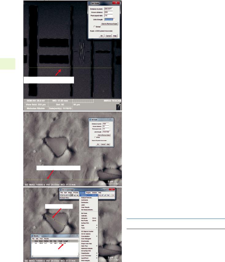
. Fig. 6.6 a ImageJ (Fiji) “Set Scale” calibration function applied to an image of NIST RM 8820. b ImageJ (Fiji) “Set Scale” calibration function applied to an image of an unknown (alloy IN100). c After “Set Scale” image calibration, subsequent use of ImageJ (Fiji) “Measure” function to determine the size of a feature of interest
different working distance (i.e., objective lens strength) is used subsequently to image the unknown specimen, the SEM software is likely to make automatic adjustments for different lens strength and scan dimensions that alter the effective magnification. For the most robust measurement environment, the user should use the calibration artifact to determine the validity of the SEM software specified scale at other working distances to develop a comprehensive calibration.
Alternatively, if the SEM magnification calibration has already been performed with an appropriate calibration artifact, then subsequent images of unknowns will be recorded with accurate dimensional information in the form of a scale bar and/or specified scan field dimensions. This information can be used with the “Set Scale” function in ImageJ-Fiji as shown for a specified field width in . Fig. 6.6b where a vector (yellow) has been chosen that spans the full image width. The “Set Scale” tool will record this length and the user then specifies the “Known Distance” and the “Unit of Length.” To minimize the effect of the uncertainty associated with selecting the endpoints when defining the scale for this image, the larger of the two dimensions reported in the vendor software was chosen, in this case the full horizontal field width of 12 μm rather than the much shorter embedded length scale of 2 μm.
Making Routine Linear Measurements
With ImageJ-Fiji (Flat Sample Placed Normal to Optic Axis)
For the case of a flat sample placed normal to the optic axis of the SEM, linear measurements of structures can be made following a simple, straightforward procedure after the image calibration procedure has been performed. Typical image- processing software tools directly available in the SEM operational software or in external software packages such as ImageJ-Fiji enable the microscopist to make simple linear measurements of objects. With the calibration established, the “Line” tool is used to define the particular linear measurement to be made, as shown in . Fig. 6.6c, and then the “Measure” tool is selected, producing the “Results” table that is shown. Repeated measurements will be accumulated in this table.
6.4\ Image Defects
6.4.1\ Projection Distortion (Foreshortening)
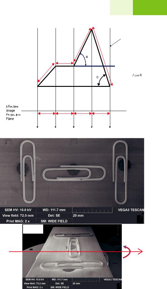
The calibration of the SEM image must be performed with the planar surface of the calibration artifact placed perpendicular to the optic axis (i.e., x- and y-axes at right angles relative to the z-axis), and only measurements that are made on planar objects that are similarly oriented will be valid. When the specimen is tilted around an axis, for example, the x-axis, the resulting SEM image is subject to projection distortion causing foreshortening along the y-axis. Foreshortening occurs because the effective magnification is reduced along the y-axis relative to the x-axis (tilt axis), as illustrated in
. Fig. 6.7. For nominal magnifications exceeding 100×, the
6.4 · Image Defects
. Fig. 6.7 a Schematic illustration of projection distortion of tilted surfaces. b Illustration of foreshortening of familiar objects, paper clips (upper) Large area image at 0 tilt; (lower) large area image at 70° tilt around a horizontal tilt axis. Note that parallel to the tilt axis, the paper clips have the same size, but perpendicular to the tilt axis severe foreshortening has occurred. The magnification also decreases significantly down the tilted surface, so the third paper clip appears smaller than the first (Images courtesy
J. Mershon, TESCAN)
|
|
|
|
99 |
6 |
a |
|
|
|
|
|
Projection |
|
|
C |
Scan Rays |
|
Distortion: |
|
|
|
||
|
|
|
|
|
|
Foreshortening |
|
|
|
D |
|
|
|
B |
|
|
|
Cross-section |
A |
|
|
|
|
through rough |
|
|
|
Strue = S* |
|
specimen |
|
|
|
|
|
|
A* |
B* |
C* |
D* |
|
|
|
|
In the SEM image, arrows spanning |
b |
|
A, B, C, D appear to be same length! |
|
|
|
||
|
|
|
|
|
|
0 tilt |
|
|
|
|
|
70º tilt
Tilt Axis
\100 Chapter 6 · Image Formation
successive scan rays of the SEM image have such a small angular spread relative to the optic axis that they create a nearly parallel projection to create the geometric mapping of the specimen three-dimensional space to the two-dimensional image space. As shown in . Fig. 6.7, a linear feature of length Ltrue lying in a plane tilted at an angle, θ, (where θ is defined relative to a plane perpendicular to the optic axis) is foreshortened in the SEM image according to the relation
Limage = Ltrue |
* |
cosθ |
\ |
(6.3) |
|
|
|
For the situation shown in . Fig. 6.7a, all four linear objects would have the same apparent size in the SEM image, but only 6 one, object B, would be shown with the correct length since it lies in a plane perpendicular to the optic axis, while the true lengths of the other linear objects would be significantly underestimated. For the most severe case, object D, which lies on the most highly tilted surface with θ= 75°, the object is a factor of 3.9 longer than it appears in the image. The effect of foreshortening is dramatically illustrated in . Fig. 6.7b, where familiar objects, paper clips, are seen in a wide area SEM image at 0° tilt and 70° tilt. At high tilt, the length of the first paper clip parallel to the tilt axis remains the same, while the second paper clip that is perpendicular to the tilt axis is highly foreshortened (Note that the third paper clip, which also lies parallel to the tilt axis, appears shorter than the first paper clip because the effective magnification decreases down the tilted surface). As shown schematically in . Fig. 6.8, foreshortening causes a square to appear as a rectangle. The effect of foreshortening is shown for an SEM image of a planar copper grid in . Fig. 6.9, where the square openings of the grid are correctly imaged at θ= 0° in . Fig. 6.9a. When the specimen
plane is tilted to θ= 45°, the grid appears to have rectangular openings, as shown in . Fig. 6.9b, with the shortened side of the true squares running parallel to the y-axis, while the correctly sized side runs parallel to the x-axis, which is the axis of tilt. Some SEMs are equipped with a “tilt correction” feature in which the y-scan perpendicular to the tilt axis is decreased to compensate for the extended length (relative to the x-scan along the tilt axis) of the scan excursion on the tilted specimen, as shown schematically in . Fig. 6.9c. Tilt correction creates the same magnification (i.e., the same pixel dimension) along orthogonal x- and y-axes, which restores the proper shape of the squares, as seen in . Fig. 6.9c. However, this scan transformation is only correct for objects that lie in the plane of the specimen. . Figure 6.9c also contains a spherical particle, which appears to be circular at θ = 0° and at θ= 45° without tilt correction, since the normal scan projects the intersection of the plane of the scan sphere as a circle.
However, when tilt correction is applied at θ = 45°, the sphere now appears to be a distorted ovoid. Thus, applying tilt correction to the image of an object with three-dimensional features of arbitrary orientation will result in image distortions that will increase in severity with the degree of local tilt.
6.4.2\ Image Defocusing (Blurring)
The act of focusing an SEM image involves adjusting the strength of the objective lens to bring the narrowest part of the focused beam cross section to be coincident with the surface. If the specimen has a flat, planar surface placed normal to the beam, then the situation illustrated in . Fig. 6.10a will exist at sufficiently low magnification. . Figure 6.10a
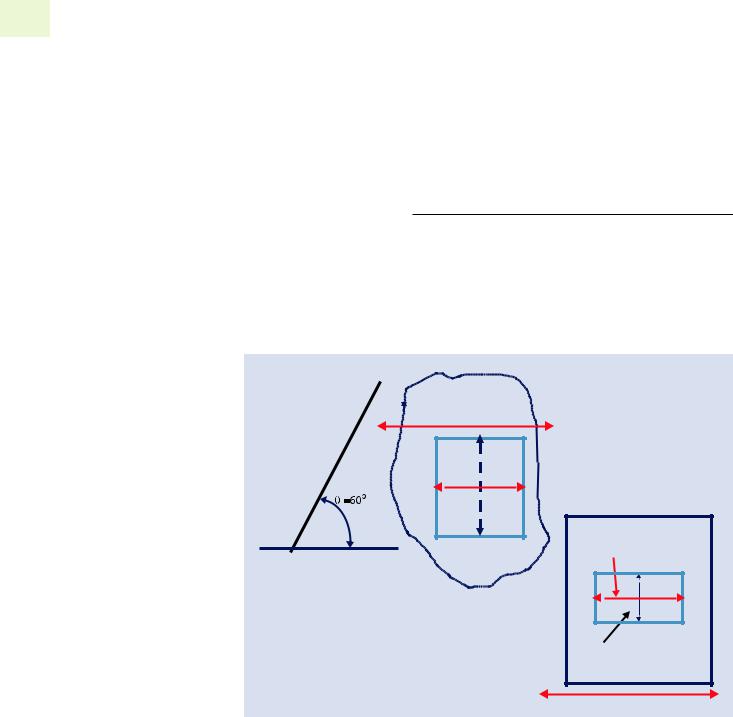
. Fig. 6.8 Effect of foreshortening of objects in a titled plane to distort square grid openings into rectangles
Tilt axis
In the SEM image, we would see
a rectangle rather than a square, with vertical dimension = horizontal * cos 60o V = 0.5 H The vertical dimension is foreshortened!
Tilt axis
How would a square object on a plane tilted to 60o from horizontal appear in the SEM image?
SEM image
True length
Foreshortened length
101 |
6 |
6.4 · Image Defects
a |
b |
c
. Fig. 6.9 a SEM/E–T (positive) image of a copper grid with a polystyrene latex sphere; tilt = 0° (grid normal to electron beam). b Grid tilted to 45°; note the effect of foreshortening distorts the square grid
openings into rectangles. c Grid tilted to 45°; “tilt correction” applied, but note that while the square grid openings are restored to the proper shape, the sphere is highly distorted
shows the locations of the beam at the pixel centers in the middle of the squares and the effective sampling footprint. The sampling footprint consists of the contribution of the incident beam diameter (in this case finely focused to a diameter <10 nm) and the surface emergence area of the BSE and SE, which is controlled by the interaction volume.
. Figure 6.10a considers a situation of a low beam energy (e.g., 5 keV) and a high atomic number (e.g., Au). For these conditions, the beam sampling footprint only occupies a
small fraction of each pixel area so that there is no possibility of overlap, i.e., sampling of adjacent pixels. Now consider what happens as the magnification is increased, i.e., the length l in Eq. (6.1) decreases while the pixel number, n, remains the same: the distance between pixel centers decreases, but the beam sampling footprint remains the same size for this particular material and beam landing energy. The situation shown in . Fig. 6.10b for the original beam sampling footprint relative to the pixel spacing and