

- •Preface
- •Imaging Microscopic Features
- •Measuring the Crystal Structure
- •References
- •Contents
- •1.4 Simulating the Effects of Elastic Scattering: Monte Carlo Calculations
- •What Are the Main Features of the Beam Electron Interaction Volume?
- •How Does the Interaction Volume Change with Composition?
- •How Does the Interaction Volume Change with Incident Beam Energy?
- •How Does the Interaction Volume Change with Specimen Tilt?
- •1.5 A Range Equation To Estimate the Size of the Interaction Volume
- •References
- •2: Backscattered Electrons
- •2.1 Origin
- •2.2.1 BSE Response to Specimen Composition (η vs. Atomic Number, Z)
- •SEM Image Contrast with BSE: “Atomic Number Contrast”
- •SEM Image Contrast: “BSE Topographic Contrast—Number Effects”
- •2.2.3 Angular Distribution of Backscattering
- •Beam Incident at an Acute Angle to the Specimen Surface (Specimen Tilt > 0°)
- •SEM Image Contrast: “BSE Topographic Contrast—Trajectory Effects”
- •2.2.4 Spatial Distribution of Backscattering
- •Depth Distribution of Backscattering
- •Radial Distribution of Backscattered Electrons
- •2.3 Summary
- •References
- •3: Secondary Electrons
- •3.1 Origin
- •3.2 Energy Distribution
- •3.3 Escape Depth of Secondary Electrons
- •3.8 Spatial Characteristics of Secondary Electrons
- •References
- •4: X-Rays
- •4.1 Overview
- •4.2 Characteristic X-Rays
- •4.2.1 Origin
- •4.2.2 Fluorescence Yield
- •4.2.3 X-Ray Families
- •4.2.4 X-Ray Nomenclature
- •4.2.6 Characteristic X-Ray Intensity
- •Isolated Atoms
- •X-Ray Production in Thin Foils
- •X-Ray Intensity Emitted from Thick, Solid Specimens
- •4.3 X-Ray Continuum (bremsstrahlung)
- •4.3.1 X-Ray Continuum Intensity
- •4.3.3 Range of X-ray Production
- •4.4 X-Ray Absorption
- •4.5 X-Ray Fluorescence
- •References
- •5.1 Electron Beam Parameters
- •5.2 Electron Optical Parameters
- •5.2.1 Beam Energy
- •Landing Energy
- •5.2.2 Beam Diameter
- •5.2.3 Beam Current
- •5.2.4 Beam Current Density
- •5.2.5 Beam Convergence Angle, α
- •5.2.6 Beam Solid Angle
- •5.2.7 Electron Optical Brightness, β
- •Brightness Equation
- •5.2.8 Focus
- •Astigmatism
- •5.3 SEM Imaging Modes
- •5.3.1 High Depth-of-Field Mode
- •5.3.2 High-Current Mode
- •5.3.3 Resolution Mode
- •5.3.4 Low-Voltage Mode
- •5.4 Electron Detectors
- •5.4.1 Important Properties of BSE and SE for Detector Design and Operation
- •Abundance
- •Angular Distribution
- •Kinetic Energy Response
- •5.4.2 Detector Characteristics
- •Angular Measures for Electron Detectors
- •Elevation (Take-Off) Angle, ψ, and Azimuthal Angle, ζ
- •Solid Angle, Ω
- •Energy Response
- •Bandwidth
- •5.4.3 Common Types of Electron Detectors
- •Backscattered Electrons
- •Passive Detectors
- •Scintillation Detectors
- •Semiconductor BSE Detectors
- •5.4.4 Secondary Electron Detectors
- •Everhart–Thornley Detector
- •Through-the-Lens (TTL) Electron Detectors
- •TTL SE Detector
- •TTL BSE Detector
- •Measuring the DQE: BSE Semiconductor Detector
- •References
- •6: Image Formation
- •6.1 Image Construction by Scanning Action
- •6.2 Magnification
- •6.3 Making Dimensional Measurements With the SEM: How Big Is That Feature?
- •Using a Calibrated Structure in ImageJ-Fiji
- •6.4 Image Defects
- •6.4.1 Projection Distortion (Foreshortening)
- •6.4.2 Image Defocusing (Blurring)
- •6.5 Making Measurements on Surfaces With Arbitrary Topography: Stereomicroscopy
- •6.5.1 Qualitative Stereomicroscopy
- •Fixed beam, Specimen Position Altered
- •Fixed Specimen, Beam Incidence Angle Changed
- •6.5.2 Quantitative Stereomicroscopy
- •Measuring a Simple Vertical Displacement
- •References
- •7: SEM Image Interpretation
- •7.1 Information in SEM Images
- •7.2.2 Calculating Atomic Number Contrast
- •Establishing a Robust Light-Optical Analogy
- •Getting It Wrong: Breaking the Light-Optical Analogy of the Everhart–Thornley (Positive Bias) Detector
- •Deconstructing the SEM/E–T Image of Topography
- •SUM Mode (A + B)
- •DIFFERENCE Mode (A−B)
- •References
- •References
- •9: Image Defects
- •9.1 Charging
- •9.1.1 What Is Specimen Charging?
- •9.1.3 Techniques to Control Charging Artifacts (High Vacuum Instruments)
- •Observing Uncoated Specimens
- •Coating an Insulating Specimen for Charge Dissipation
- •Choosing the Coating for Imaging Morphology
- •9.2 Radiation Damage
- •9.3 Contamination
- •References
- •10: High Resolution Imaging
- •10.2 Instrumentation Considerations
- •10.4.1 SE Range Effects Produce Bright Edges (Isolated Edges)
- •10.4.4 Too Much of a Good Thing: The Bright Edge Effect Hinders Locating the True Position of an Edge for Critical Dimension Metrology
- •10.5.1 Beam Energy Strategies
- •Low Beam Energy Strategy
- •High Beam Energy Strategy
- •Making More SE1: Apply a Thin High-δ Metal Coating
- •Making Fewer BSEs, SE2, and SE3 by Eliminating Bulk Scattering From the Substrate
- •10.6 Factors That Hinder Achieving High Resolution
- •10.6.2 Pathological Specimen Behavior
- •Contamination
- •Instabilities
- •References
- •11: Low Beam Energy SEM
- •11.3 Selecting the Beam Energy to Control the Spatial Sampling of Imaging Signals
- •11.3.1 Low Beam Energy for High Lateral Resolution SEM
- •11.3.2 Low Beam Energy for High Depth Resolution SEM
- •11.3.3 Extremely Low Beam Energy Imaging
- •References
- •12.1.1 Stable Electron Source Operation
- •12.1.2 Maintaining Beam Integrity
- •12.1.4 Minimizing Contamination
- •12.3.1 Control of Specimen Charging
- •12.5 VPSEM Image Resolution
- •References
- •13: ImageJ and Fiji
- •13.1 The ImageJ Universe
- •13.2 Fiji
- •13.3 Plugins
- •13.4 Where to Learn More
- •References
- •14: SEM Imaging Checklist
- •14.1.1 Conducting or Semiconducting Specimens
- •14.1.2 Insulating Specimens
- •14.2 Electron Signals Available
- •14.2.1 Beam Electron Range
- •14.2.2 Backscattered Electrons
- •14.2.3 Secondary Electrons
- •14.3 Selecting the Electron Detector
- •14.3.2 Backscattered Electron Detectors
- •14.3.3 “Through-the-Lens” Detectors
- •14.4 Selecting the Beam Energy for SEM Imaging
- •14.4.4 High Resolution SEM Imaging
- •Strategy 1
- •Strategy 2
- •14.5 Selecting the Beam Current
- •14.5.1 High Resolution Imaging
- •14.5.2 Low Contrast Features Require High Beam Current and/or Long Frame Time to Establish Visibility
- •14.6 Image Presentation
- •14.6.1 “Live” Display Adjustments
- •14.6.2 Post-Collection Processing
- •14.7 Image Interpretation
- •14.7.1 Observer’s Point of View
- •14.7.3 Contrast Encoding
- •14.8.1 VPSEM Advantages
- •14.8.2 VPSEM Disadvantages
- •15: SEM Case Studies
- •15.1 Case Study: How High Is That Feature Relative to Another?
- •15.2 Revealing Shallow Surface Relief
- •16.1.2 Minor Artifacts: The Si-Escape Peak
- •16.1.3 Minor Artifacts: Coincidence Peaks
- •16.1.4 Minor Artifacts: Si Absorption Edge and Si Internal Fluorescence Peak
- •16.2 “Best Practices” for Electron-Excited EDS Operation
- •16.2.1 Operation of the EDS System
- •Choosing the EDS Time Constant (Resolution and Throughput)
- •Choosing the Solid Angle of the EDS
- •Selecting a Beam Current for an Acceptable Level of System Dead-Time
- •16.3.1 Detector Geometry
- •16.3.2 Process Time
- •16.3.3 Optimal Working Distance
- •16.3.4 Detector Orientation
- •16.3.5 Count Rate Linearity
- •16.3.6 Energy Calibration Linearity
- •16.3.7 Other Items
- •16.3.8 Setting Up a Quality Control Program
- •Using the QC Tools Within DTSA-II
- •Creating a QC Project
- •Linearity of Output Count Rate with Live-Time Dose
- •Resolution and Peak Position Stability with Count Rate
- •Solid Angle for Low X-ray Flux
- •Maximizing Throughput at Moderate Resolution
- •References
- •17: DTSA-II EDS Software
- •17.1 Getting Started With NIST DTSA-II
- •17.1.1 Motivation
- •17.1.2 Platform
- •17.1.3 Overview
- •17.1.4 Design
- •Simulation
- •Quantification
- •Experiment Design
- •Modeled Detectors (. Fig. 17.1)
- •Window Type (. Fig. 17.2)
- •The Optimal Working Distance (. Figs. 17.3 and 17.4)
- •Elevation Angle
- •Sample-to-Detector Distance
- •Detector Area
- •Crystal Thickness
- •Number of Channels, Energy Scale, and Zero Offset
- •Resolution at Mn Kα (Approximate)
- •Azimuthal Angle
- •Gold Layer, Aluminum Layer, Nickel Layer
- •Dead Layer
- •Zero Strobe Discriminator (. Figs. 17.7 and 17.8)
- •Material Editor Dialog (. Figs. 17.9, 17.10, 17.11, 17.12, 17.13, and 17.14)
- •17.2.1 Introduction
- •17.2.2 Monte Carlo Simulation
- •17.2.4 Optional Tables
- •References
- •18: Qualitative Elemental Analysis by Energy Dispersive X-Ray Spectrometry
- •18.1 Quality Assurance Issues for Qualitative Analysis: EDS Calibration
- •18.2 Principles of Qualitative EDS Analysis
- •Exciting Characteristic X-Rays
- •Fluorescence Yield
- •X-ray Absorption
- •Si Escape Peak
- •Coincidence Peaks
- •18.3 Performing Manual Qualitative Analysis
- •Beam Energy
- •Choosing the EDS Resolution (Detector Time Constant)
- •Obtaining Adequate Counts
- •18.4.1 Employ the Available Software Tools
- •18.4.3 Lower Photon Energy Region
- •18.4.5 Checking Your Work
- •18.5 A Worked Example of Manual Peak Identification
- •References
- •19.1 What Is a k-ratio?
- •19.3 Sets of k-ratios
- •19.5 The Analytical Total
- •19.6 Normalization
- •19.7.1 Oxygen by Assumed Stoichiometry
- •19.7.3 Element by Difference
- •19.8 Ways of Reporting Composition
- •19.8.1 Mass Fraction
- •19.8.2 Atomic Fraction
- •19.8.3 Stoichiometry
- •19.8.4 Oxide Fractions
- •Example Calculations
- •19.9 The Accuracy of Quantitative Electron-Excited X-ray Microanalysis
- •19.9.1 Standards-Based k-ratio Protocol
- •19.9.2 “Standardless Analysis”
- •19.10 Appendix
- •19.10.1 The Need for Matrix Corrections To Achieve Quantitative Analysis
- •19.10.2 The Physical Origin of Matrix Effects
- •19.10.3 ZAF Factors in Microanalysis
- •X-ray Generation With Depth, φ(ρz)
- •X-ray Absorption Effect, A
- •X-ray Fluorescence, F
- •References
- •20.2 Instrumentation Requirements
- •20.2.1 Choosing the EDS Parameters
- •EDS Spectrum Channel Energy Width and Spectrum Energy Span
- •EDS Time Constant (Resolution and Throughput)
- •EDS Calibration
- •EDS Solid Angle
- •20.2.2 Choosing the Beam Energy, E0
- •20.2.3 Measuring the Beam Current
- •20.2.4 Choosing the Beam Current
- •Optimizing Analysis Strategy
- •20.3.4 Ba-Ti Interference in BaTiSi3O9
- •20.4 The Need for an Iterative Qualitative and Quantitative Analysis Strategy
- •20.4.2 Analysis of a Stainless Steel
- •20.5 Is the Specimen Homogeneous?
- •20.6 Beam-Sensitive Specimens
- •20.6.1 Alkali Element Migration
- •20.6.2 Materials Subject to Mass Loss During Electron Bombardment—the Marshall-Hall Method
- •Thin Section Analysis
- •Bulk Biological and Organic Specimens
- •References
- •21: Trace Analysis by SEM/EDS
- •21.1 Limits of Detection for SEM/EDS Microanalysis
- •21.2.1 Estimating CDL from a Trace or Minor Constituent from Measuring a Known Standard
- •21.2.2 Estimating CDL After Determination of a Minor or Trace Constituent with Severe Peak Interference from a Major Constituent
- •21.3 Measurements of Trace Constituents by Electron-Excited Energy Dispersive X-ray Spectrometry
- •The Inevitable Physics of Remote Excitation Within the Specimen: Secondary Fluorescence Beyond the Electron Interaction Volume
- •Simulation of Long-Range Secondary X-ray Fluorescence
- •NIST DTSA II Simulation: Vertical Interface Between Two Regions of Different Composition in a Flat Bulk Target
- •NIST DTSA II Simulation: Cubic Particle Embedded in a Bulk Matrix
- •21.5 Summary
- •References
- •22.1.2 Low Beam Energy Analysis Range
- •22.2 Advantage of Low Beam Energy X-Ray Microanalysis
- •22.2.1 Improved Spatial Resolution
- •22.3 Challenges and Limitations of Low Beam Energy X-Ray Microanalysis
- •22.3.1 Reduced Access to Elements
- •22.3.3 At Low Beam Energy, Almost Everything Is Found To Be Layered
- •Analysis of Surface Contamination
- •References
- •23: Analysis of Specimens with Special Geometry: Irregular Bulk Objects and Particles
- •23.2.1 No Chemical Etching
- •23.3 Consequences of Attempting Analysis of Bulk Materials With Rough Surfaces
- •23.4.1 The Raw Analytical Total
- •23.4.2 The Shape of the EDS Spectrum
- •23.5 Best Practices for Analysis of Rough Bulk Samples
- •23.6 Particle Analysis
- •Particle Sample Preparation: Bulk Substrate
- •The Importance of Beam Placement
- •Overscanning
- •“Particle Mass Effect”
- •“Particle Absorption Effect”
- •The Analytical Total Reveals the Impact of Particle Effects
- •Does Overscanning Help?
- •23.6.6 Peak-to-Background (P/B) Method
- •Specimen Geometry Severely Affects the k-ratio, but Not the P/B
- •Using the P/B Correspondence
- •23.7 Summary
- •References
- •24: Compositional Mapping
- •24.2 X-Ray Spectrum Imaging
- •24.2.1 Utilizing XSI Datacubes
- •24.2.2 Derived Spectra
- •SUM Spectrum
- •MAXIMUM PIXEL Spectrum
- •24.3 Quantitative Compositional Mapping
- •24.4 Strategy for XSI Elemental Mapping Data Collection
- •24.4.1 Choosing the EDS Dead-Time
- •24.4.2 Choosing the Pixel Density
- •24.4.3 Choosing the Pixel Dwell Time
- •“Flash Mapping”
- •High Count Mapping
- •References
- •25.1 Gas Scattering Effects in the VPSEM
- •25.1.1 Why Doesn’t the EDS Collimator Exclude the Remote Skirt X-Rays?
- •25.2 What Can Be Done To Minimize gas Scattering in VPSEM?
- •25.2.2 Favorable Sample Characteristics
- •Particle Analysis
- •25.2.3 Unfavorable Sample Characteristics
- •References
- •26.1 Instrumentation
- •26.1.2 EDS Detector
- •26.1.3 Probe Current Measurement Device
- •Direct Measurement: Using a Faraday Cup and Picoammeter
- •A Faraday Cup
- •Electrically Isolated Stage
- •Indirect Measurement: Using a Calibration Spectrum
- •26.1.4 Conductive Coating
- •26.2 Sample Preparation
- •26.2.1 Standard Materials
- •26.2.2 Peak Reference Materials
- •26.3 Initial Set-Up
- •26.3.1 Calibrating the EDS Detector
- •Selecting a Pulse Process Time Constant
- •Energy Calibration
- •Quality Control
- •Sample Orientation
- •Detector Position
- •Probe Current
- •26.4 Collecting Data
- •26.4.1 Exploratory Spectrum
- •26.4.2 Experiment Optimization
- •26.4.3 Selecting Standards
- •26.4.4 Reference Spectra
- •26.4.5 Collecting Standards
- •26.4.6 Collecting Peak-Fitting References
- •26.5 Data Analysis
- •26.5.2 Quantification
- •26.6 Quality Check
- •Reference
- •27.2 Case Study: Aluminum Wire Failures in Residential Wiring
- •References
- •28: Cathodoluminescence
- •28.1 Origin
- •28.2 Measuring Cathodoluminescence
- •28.3 Applications of CL
- •28.3.1 Geology
- •Carbonado Diamond
- •Ancient Impact Zircons
- •28.3.2 Materials Science
- •Semiconductors
- •Lead-Acid Battery Plate Reactions
- •28.3.3 Organic Compounds
- •References
- •29.1.1 Single Crystals
- •29.1.2 Polycrystalline Materials
- •29.1.3 Conditions for Detecting Electron Channeling Contrast
- •Specimen Preparation
- •Instrument Conditions
- •29.2.1 Origin of EBSD Patterns
- •29.2.2 Cameras for EBSD Pattern Detection
- •29.2.3 EBSD Spatial Resolution
- •29.2.5 Steps in Typical EBSD Measurements
- •Sample Preparation for EBSD
- •Align Sample in the SEM
- •Check for EBSD Patterns
- •Adjust SEM and Select EBSD Map Parameters
- •Run the Automated Map
- •29.2.6 Display of the Acquired Data
- •29.2.7 Other Map Components
- •29.2.10 Application Example
- •Application of EBSD To Understand Meteorite Formation
- •29.2.11 Summary
- •Specimen Considerations
- •EBSD Detector
- •Selection of Candidate Crystallographic Phases
- •Microscope Operating Conditions and Pattern Optimization
- •Selection of EBSD Acquisition Parameters
- •Collect the Orientation Map
- •References
- •30.1 Introduction
- •30.2 Ion–Solid Interactions
- •30.3 Focused Ion Beam Systems
- •30.5 Preparation of Samples for SEM
- •30.5.1 Cross-Section Preparation
- •30.5.2 FIB Sample Preparation for 3D Techniques and Imaging
- •30.6 Summary
- •References
- •31: Ion Beam Microscopy
- •31.1 What Is So Useful About Ions?
- •31.2 Generating Ion Beams
- •31.3 Signal Generation in the HIM
- •31.5 Patterning with Ion Beams
- •31.7 Chemical Microanalysis with Ion Beams
- •References
- •Appendix
- •A Database of Electron–Solid Interactions
- •A Database of Electron–Solid Interactions
- •Introduction
- •Backscattered Electrons
- •Secondary Yields
- •Stopping Powers
- •X-ray Ionization Cross Sections
- •Conclusions
- •References
- •Index
- •Reference List
- •Index

413 |
|
24 |
|
|
|
Compositional Mapping
24.1\ Total Intensity Region-of-Interest Mapping – 414
24.1.1\ Limitations of Total Intensity Mapping – 415
24.2\ X-Ray Spectrum Imaging – 417
24.2.1\ Utilizing XSI Datacubes – 419
24.2.2\ Derived Spectra – 419
24.3\ Quantitative Compositional Mapping – 424
24.4\ Strategy for XSI Elemental Mapping Data Collection – 430
24.4.1\ Choosing the EDS Dead-Time – 430 24.4.2\ Choosing the Pixel Density – 432 24.4.3\ Choosing the Pixel Dwell Time – 434
References – 439
© Springer Science+Business Media LLC 2018
J. Goldstein et al., Scanning Electron Microscopy and X-Ray Microanalysis, https://doi.org/10.1007/978-1-4939-6676-9_24
\414 Chapter 24 · Compositional Mapping
SEM images that show the spatial distribution of the elemental constituents of a specimen (“elemental maps”) can be created by using the characteristic X-ray intensity measured for each element with the energy dispersive X-ray spectrometer (EDS) to define the gray level (or color value) at each picture element (pixel) of the scan. Elemental maps based on X-ray intensity provide qualitative information on spatial distributions of elements. Compositional mapping, in which a full EDS spectrum is recorded at each pixel (“X-ray Spectrum Imaging” or XSI) and processed with peak fitting, k-ratio standardization, and matrix corrections, provides a quantitative basis for comparing maps of different elements in the same region, or for the same element from different regions.
24.1\ Total Intensity Region-of-Interest
Mapping
In the simplest implementation of elemental mapping, energy regions are defined in the spectrum that span the characteristic X-ray peak(s) of interest, as shown in
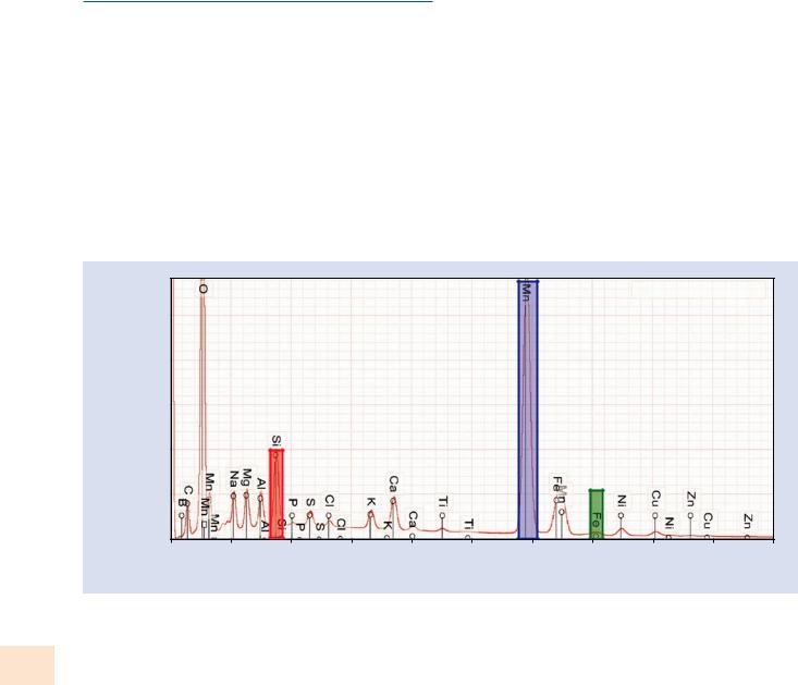
. Fig. 24.1. The total X-ray intensity (counts) within each energy region, IXi, consisting of both the characteristic peak intensity, including any overlapping peaks, and the continuum background intensity, is digitally recorded for each pixel, creating a set of x-y-IXi image arrays for the defined suite of elements. Depending on the local concentration of an element, the overvoltage U0 = E0/Ec for the measured characteristic peak, the beam current, the solid angle of the detector, and the dwell time per pixel, the number of counts
per elemental window can vary widely from a few counts per pixel to several thousand or more. A typical strategy to avoid saturation is to collect 2-byte deep X-ray intensity data that permits up to 65,536 counts per energy region per pixel. In common with the practice for BSE and SE images, the final elemental map will be displayed with a 1-byte intensity range (0–255 gray levels). To maximize the contrast within each map it is necessary to nearly fill this display range so that it is common practice to automatically scale (“autoscale”) the measured intensity in a linear fashion to span slightly less than 1-byte. The displayed gray levels are scaled to range from near black, but avoiding black (gray level zero) to avoid clipping, to near white, but avoiding full white (gray level 255), to prevent saturation. The counts are expanded for elements that span less than 1-byte in the original data collection, while the counts are compressed for elements that extend into the 2-byte range. An example of such total intensity mapping is shown in . Fig. 24.2, which presents a set of maps for Si, Fe, and Mn in a cross section of a deep-sea manganese nodule with a complex microstructure. The EDS spectrum shown in . Fig. 24.1 also reveals a typical problem encountered in simple intensity window mapping. Manganese is one of the most abundant elements in this specimen, and the Mn K-M2,3 (6.490 keV) interferes with Fe K-L2,3 (6.400 keV), which is especially significant since iron is a minor/trace constituent. To avoid the potential artifacts in this situation, the analyst can instead choose
the Fe K-M2,3 (7.057 keV) which does not suffer the interference but which is approximately a factor of ten lower
intensity than Fe K-L2,3. While sacrificing sensitivity, the
Counts
1000000
800000
600000
400000
200000
0
0.0
Mn |
|
Mn-nodule_20kV25nA |
|
|
Si
Fe
1.0 |
2.0 |
3.0 |
4.0 |
5.0 |
6.0 |
7.0 |
8.0 |
9.0 |
10.0 |
|
|
|
Photon energy (KeV) |
|
|
|
|
|
|
. Fig. 24.1 EDS spectrum measured on a cross section of a deep-sea manganese nodule showing peak selection (Si K-L2, Mn K-L2,3, and Fe K-M2,3) for total intensity elemental mapping
24
415 |
24 |
24.1 · Total Intensity Region-of-Interest Mapping
Si |
Fe |
20 µm
Mn |
Si Fe Mn |
|
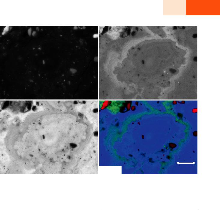
. Fig. 24.2 Total intensity elemental maps for Si K-L2, Mn K-L2,3, and Fe K-M2,3 measured on a cross section of a deep-sea manganese nodule, and the color overlay of the gray-scale maps
success of this strategy is revealed in . Fig. 24.2, where the major Mn and minor Fe are seen to be anti-correlated.
. Figure 24.2 also contains a primary color overlay of these three elements, encoded with Si in red, Fe in green, and Mn in blue, a commonly used image display tool which provides an immediate visual comparison of the relative spatial relationships of the three constituents. The appearance of secondary colors shows areas of coincidence of any two elements, for example, the cyan colored region is a combination of green and blue and thus shows the coincidence of Fe and Mn. The other possible binary combinations are yellow (red plus green, Si + Fe) and magenta (red plus blue, Si + Mn), which are not present in this example. If all three elements were present at the same location, white would result.
24.1.1\ Limitations of Total Intensity
Mapping
While total intensity elemental maps such as those in
. Fig. 24.2 are useful for developing a basic understanding of the spatial distributions of the elements that make up the specimen, total intensity mapping is subject to several significant limitations:
\1.\ By selecting only the spectral regions-of-interest, the amount of mass storage is minimized. However, while all spectral regions-of-interest are collected simultaneously, if the analyst needs to evaluate another element not ori ginally selected when the data was collected, the entire image scan must be repeated to recollect the data with that new element included.

\416 Chapter 24 · Compositional Mapping
\2.\ Total intensity maps convey qualitative information only. The elemental spatial distributions are meaningful only in qualitative terms of interpreting which elements are present at a particular pixel location(s) by comparing different elemental maps of the same area, for example, using the color overlay method. Since the images are recorded simultaneously, the pixel registration is without error even if overall drift or other distortion occurs. However, the intensity information is not quantitative and can only convey relative abundance information within an individual elemental map (e.g., “this location has more of element A than this location because the intensity of A is higher”). The gray levels in maps for different elements cannot be readily compared because the X-ray intensity for each element that defines the gray level range of the map is determined by the local concentration and the complex physics of X-ray generation, propagation, and detection efficiency, all of which vary with the elemental species. The element-to-element differences in the efficiency of X-ray production, propagation, and detection are embedded in the raw measured X-ray intensities, which are then subjected to the autoscaling operation. Unless the autoscaling factor is recorded (typically not), it is not possible after the fact to recover the information that would enable the analyst to standardize and establish a proper basis for inter-comparison of maps of different elements, or even of maps of the same element from different areas. Thus, the sequence of gray levels only has interpretable meaning within an individual elemental map. Gray levels cannot be sensibly compared between total intensity maps of different elements, for example, the near-white level in the autoscaled maps of . Fig. 24.2 for Si, Fe, and Mn does not correspond to the same X-ray intensity or concentration for three elements. Because of autoscaling, it is not possible to compare maps for the same element “A” from two different regions, even if recorded with the same dose conditions, since the autoscaling factor will be controlled by the maximum concentration of “A,” which may not be the same in two arbitrarily chosen regions of the sample.
\3.\ This lack of quantitative information in elemental total intensity maps extends to the color overlay presentation of elemental maps seen in . Fig. 24.2. The color overlay is useful to compare the spatial relationships among the three elements, but the specific color observed
at any pixel only depicts elemental coincidence not absolute or relative concentration. The particular color that occurs at a given pixel depends on the complex physics of X-ray generation, propagation, and detection as well as concentration, and the autoscaling of the separate maps that precedes the color overlay, which distorts the apparent relationships among the elemental constituents, also influences the observed colors.
\4.\ When peak interference occurs, the raw intensity in a given energy window may contain contributions from another element, as shown in . Fig. 24.1 where the region that includes Fe K-L2,3 also contains intensity from Mn K-M2,3. While choosing the non-interfered peak Fe K-M2,3 gives a useful result in the case of the manganese nodule, if the specimen also contained cobalt at a significant level, Co K-L2,3 (6.930 keV) would interfere with Fe K-M2,3 (7.057 keV) and invalidate this strategy. The peak
interference artifact can be corrected by peak fitting,
or by methods in which the measured Mn K-L2,3 intensity, which does not suffer interference in this
particular case, is used to correct the intensity of the
Fe K-L2,3 + Mn K-M2,3 window using the known Mn K-M2,3/K-L2,3 ratio.
\5.\ The total intensity window contains both the characteristic peak intensity that is specific to an element and the continuum (background) intensity, which scales with the average atomic number of all of the elements within the excited interaction volume but is not exclusively related to the element that is generating the peak. For the map of an element that constitutes a major constituent (mass concentration C >0.1 or 10 wt %), the non-specific background intensity contribution usually does not constitute a serious mapping artifact. However, for a minor constituent (0.01 ≤ C ≤ 0.1, 1 wt % to 10 wt %), the average atomic number dependence of the continuum background can lead to serious artifacts. . Figure 24.3 shows an example of this phenomenon for a Raney nickel alloy containing major Al and Ni with minor Fe. The complex microstructure has four distinct phases, the compositions of which are listed in . Table 24.1, one of which contains Fe as a minor constituent at a concentration of approximately C = 0.04 (4 wt %). This Fe-rich phase can be readily discerned in the Fe gray-scale map, where the intensity of this phase, being the highest iron-containing region in the image, has been autoscaled to near white. In addition to this Fe-containing phase, there appears to be segregation of lower concentration levels of Fe to the Ni-rich phase relative to the Al-rich phase. However, this effect is at least partially due to the increase in the continuum background in the Ni-rich region relative to the Al-rich region because of the sharp difference in the average atomic number. For trace constituents (C < 0.01, 1 wt %), the atomic number dependence of the continuum background can dominate the observed contrast, creating artifacts in the images that render most trace constituent maps nearly useless.
24