

- •Preface
- •Imaging Microscopic Features
- •Measuring the Crystal Structure
- •References
- •Contents
- •1.4 Simulating the Effects of Elastic Scattering: Monte Carlo Calculations
- •What Are the Main Features of the Beam Electron Interaction Volume?
- •How Does the Interaction Volume Change with Composition?
- •How Does the Interaction Volume Change with Incident Beam Energy?
- •How Does the Interaction Volume Change with Specimen Tilt?
- •1.5 A Range Equation To Estimate the Size of the Interaction Volume
- •References
- •2: Backscattered Electrons
- •2.1 Origin
- •2.2.1 BSE Response to Specimen Composition (η vs. Atomic Number, Z)
- •SEM Image Contrast with BSE: “Atomic Number Contrast”
- •SEM Image Contrast: “BSE Topographic Contrast—Number Effects”
- •2.2.3 Angular Distribution of Backscattering
- •Beam Incident at an Acute Angle to the Specimen Surface (Specimen Tilt > 0°)
- •SEM Image Contrast: “BSE Topographic Contrast—Trajectory Effects”
- •2.2.4 Spatial Distribution of Backscattering
- •Depth Distribution of Backscattering
- •Radial Distribution of Backscattered Electrons
- •2.3 Summary
- •References
- •3: Secondary Electrons
- •3.1 Origin
- •3.2 Energy Distribution
- •3.3 Escape Depth of Secondary Electrons
- •3.8 Spatial Characteristics of Secondary Electrons
- •References
- •4: X-Rays
- •4.1 Overview
- •4.2 Characteristic X-Rays
- •4.2.1 Origin
- •4.2.2 Fluorescence Yield
- •4.2.3 X-Ray Families
- •4.2.4 X-Ray Nomenclature
- •4.2.6 Characteristic X-Ray Intensity
- •Isolated Atoms
- •X-Ray Production in Thin Foils
- •X-Ray Intensity Emitted from Thick, Solid Specimens
- •4.3 X-Ray Continuum (bremsstrahlung)
- •4.3.1 X-Ray Continuum Intensity
- •4.3.3 Range of X-ray Production
- •4.4 X-Ray Absorption
- •4.5 X-Ray Fluorescence
- •References
- •5.1 Electron Beam Parameters
- •5.2 Electron Optical Parameters
- •5.2.1 Beam Energy
- •Landing Energy
- •5.2.2 Beam Diameter
- •5.2.3 Beam Current
- •5.2.4 Beam Current Density
- •5.2.5 Beam Convergence Angle, α
- •5.2.6 Beam Solid Angle
- •5.2.7 Electron Optical Brightness, β
- •Brightness Equation
- •5.2.8 Focus
- •Astigmatism
- •5.3 SEM Imaging Modes
- •5.3.1 High Depth-of-Field Mode
- •5.3.2 High-Current Mode
- •5.3.3 Resolution Mode
- •5.3.4 Low-Voltage Mode
- •5.4 Electron Detectors
- •5.4.1 Important Properties of BSE and SE for Detector Design and Operation
- •Abundance
- •Angular Distribution
- •Kinetic Energy Response
- •5.4.2 Detector Characteristics
- •Angular Measures for Electron Detectors
- •Elevation (Take-Off) Angle, ψ, and Azimuthal Angle, ζ
- •Solid Angle, Ω
- •Energy Response
- •Bandwidth
- •5.4.3 Common Types of Electron Detectors
- •Backscattered Electrons
- •Passive Detectors
- •Scintillation Detectors
- •Semiconductor BSE Detectors
- •5.4.4 Secondary Electron Detectors
- •Everhart–Thornley Detector
- •Through-the-Lens (TTL) Electron Detectors
- •TTL SE Detector
- •TTL BSE Detector
- •Measuring the DQE: BSE Semiconductor Detector
- •References
- •6: Image Formation
- •6.1 Image Construction by Scanning Action
- •6.2 Magnification
- •6.3 Making Dimensional Measurements With the SEM: How Big Is That Feature?
- •Using a Calibrated Structure in ImageJ-Fiji
- •6.4 Image Defects
- •6.4.1 Projection Distortion (Foreshortening)
- •6.4.2 Image Defocusing (Blurring)
- •6.5 Making Measurements on Surfaces With Arbitrary Topography: Stereomicroscopy
- •6.5.1 Qualitative Stereomicroscopy
- •Fixed beam, Specimen Position Altered
- •Fixed Specimen, Beam Incidence Angle Changed
- •6.5.2 Quantitative Stereomicroscopy
- •Measuring a Simple Vertical Displacement
- •References
- •7: SEM Image Interpretation
- •7.1 Information in SEM Images
- •7.2.2 Calculating Atomic Number Contrast
- •Establishing a Robust Light-Optical Analogy
- •Getting It Wrong: Breaking the Light-Optical Analogy of the Everhart–Thornley (Positive Bias) Detector
- •Deconstructing the SEM/E–T Image of Topography
- •SUM Mode (A + B)
- •DIFFERENCE Mode (A−B)
- •References
- •References
- •9: Image Defects
- •9.1 Charging
- •9.1.1 What Is Specimen Charging?
- •9.1.3 Techniques to Control Charging Artifacts (High Vacuum Instruments)
- •Observing Uncoated Specimens
- •Coating an Insulating Specimen for Charge Dissipation
- •Choosing the Coating for Imaging Morphology
- •9.2 Radiation Damage
- •9.3 Contamination
- •References
- •10: High Resolution Imaging
- •10.2 Instrumentation Considerations
- •10.4.1 SE Range Effects Produce Bright Edges (Isolated Edges)
- •10.4.4 Too Much of a Good Thing: The Bright Edge Effect Hinders Locating the True Position of an Edge for Critical Dimension Metrology
- •10.5.1 Beam Energy Strategies
- •Low Beam Energy Strategy
- •High Beam Energy Strategy
- •Making More SE1: Apply a Thin High-δ Metal Coating
- •Making Fewer BSEs, SE2, and SE3 by Eliminating Bulk Scattering From the Substrate
- •10.6 Factors That Hinder Achieving High Resolution
- •10.6.2 Pathological Specimen Behavior
- •Contamination
- •Instabilities
- •References
- •11: Low Beam Energy SEM
- •11.3 Selecting the Beam Energy to Control the Spatial Sampling of Imaging Signals
- •11.3.1 Low Beam Energy for High Lateral Resolution SEM
- •11.3.2 Low Beam Energy for High Depth Resolution SEM
- •11.3.3 Extremely Low Beam Energy Imaging
- •References
- •12.1.1 Stable Electron Source Operation
- •12.1.2 Maintaining Beam Integrity
- •12.1.4 Minimizing Contamination
- •12.3.1 Control of Specimen Charging
- •12.5 VPSEM Image Resolution
- •References
- •13: ImageJ and Fiji
- •13.1 The ImageJ Universe
- •13.2 Fiji
- •13.3 Plugins
- •13.4 Where to Learn More
- •References
- •14: SEM Imaging Checklist
- •14.1.1 Conducting or Semiconducting Specimens
- •14.1.2 Insulating Specimens
- •14.2 Electron Signals Available
- •14.2.1 Beam Electron Range
- •14.2.2 Backscattered Electrons
- •14.2.3 Secondary Electrons
- •14.3 Selecting the Electron Detector
- •14.3.2 Backscattered Electron Detectors
- •14.3.3 “Through-the-Lens” Detectors
- •14.4 Selecting the Beam Energy for SEM Imaging
- •14.4.4 High Resolution SEM Imaging
- •Strategy 1
- •Strategy 2
- •14.5 Selecting the Beam Current
- •14.5.1 High Resolution Imaging
- •14.5.2 Low Contrast Features Require High Beam Current and/or Long Frame Time to Establish Visibility
- •14.6 Image Presentation
- •14.6.1 “Live” Display Adjustments
- •14.6.2 Post-Collection Processing
- •14.7 Image Interpretation
- •14.7.1 Observer’s Point of View
- •14.7.3 Contrast Encoding
- •14.8.1 VPSEM Advantages
- •14.8.2 VPSEM Disadvantages
- •15: SEM Case Studies
- •15.1 Case Study: How High Is That Feature Relative to Another?
- •15.2 Revealing Shallow Surface Relief
- •16.1.2 Minor Artifacts: The Si-Escape Peak
- •16.1.3 Minor Artifacts: Coincidence Peaks
- •16.1.4 Minor Artifacts: Si Absorption Edge and Si Internal Fluorescence Peak
- •16.2 “Best Practices” for Electron-Excited EDS Operation
- •16.2.1 Operation of the EDS System
- •Choosing the EDS Time Constant (Resolution and Throughput)
- •Choosing the Solid Angle of the EDS
- •Selecting a Beam Current for an Acceptable Level of System Dead-Time
- •16.3.1 Detector Geometry
- •16.3.2 Process Time
- •16.3.3 Optimal Working Distance
- •16.3.4 Detector Orientation
- •16.3.5 Count Rate Linearity
- •16.3.6 Energy Calibration Linearity
- •16.3.7 Other Items
- •16.3.8 Setting Up a Quality Control Program
- •Using the QC Tools Within DTSA-II
- •Creating a QC Project
- •Linearity of Output Count Rate with Live-Time Dose
- •Resolution and Peak Position Stability with Count Rate
- •Solid Angle for Low X-ray Flux
- •Maximizing Throughput at Moderate Resolution
- •References
- •17: DTSA-II EDS Software
- •17.1 Getting Started With NIST DTSA-II
- •17.1.1 Motivation
- •17.1.2 Platform
- •17.1.3 Overview
- •17.1.4 Design
- •Simulation
- •Quantification
- •Experiment Design
- •Modeled Detectors (. Fig. 17.1)
- •Window Type (. Fig. 17.2)
- •The Optimal Working Distance (. Figs. 17.3 and 17.4)
- •Elevation Angle
- •Sample-to-Detector Distance
- •Detector Area
- •Crystal Thickness
- •Number of Channels, Energy Scale, and Zero Offset
- •Resolution at Mn Kα (Approximate)
- •Azimuthal Angle
- •Gold Layer, Aluminum Layer, Nickel Layer
- •Dead Layer
- •Zero Strobe Discriminator (. Figs. 17.7 and 17.8)
- •Material Editor Dialog (. Figs. 17.9, 17.10, 17.11, 17.12, 17.13, and 17.14)
- •17.2.1 Introduction
- •17.2.2 Monte Carlo Simulation
- •17.2.4 Optional Tables
- •References
- •18: Qualitative Elemental Analysis by Energy Dispersive X-Ray Spectrometry
- •18.1 Quality Assurance Issues for Qualitative Analysis: EDS Calibration
- •18.2 Principles of Qualitative EDS Analysis
- •Exciting Characteristic X-Rays
- •Fluorescence Yield
- •X-ray Absorption
- •Si Escape Peak
- •Coincidence Peaks
- •18.3 Performing Manual Qualitative Analysis
- •Beam Energy
- •Choosing the EDS Resolution (Detector Time Constant)
- •Obtaining Adequate Counts
- •18.4.1 Employ the Available Software Tools
- •18.4.3 Lower Photon Energy Region
- •18.4.5 Checking Your Work
- •18.5 A Worked Example of Manual Peak Identification
- •References
- •19.1 What Is a k-ratio?
- •19.3 Sets of k-ratios
- •19.5 The Analytical Total
- •19.6 Normalization
- •19.7.1 Oxygen by Assumed Stoichiometry
- •19.7.3 Element by Difference
- •19.8 Ways of Reporting Composition
- •19.8.1 Mass Fraction
- •19.8.2 Atomic Fraction
- •19.8.3 Stoichiometry
- •19.8.4 Oxide Fractions
- •Example Calculations
- •19.9 The Accuracy of Quantitative Electron-Excited X-ray Microanalysis
- •19.9.1 Standards-Based k-ratio Protocol
- •19.9.2 “Standardless Analysis”
- •19.10 Appendix
- •19.10.1 The Need for Matrix Corrections To Achieve Quantitative Analysis
- •19.10.2 The Physical Origin of Matrix Effects
- •19.10.3 ZAF Factors in Microanalysis
- •X-ray Generation With Depth, φ(ρz)
- •X-ray Absorption Effect, A
- •X-ray Fluorescence, F
- •References
- •20.2 Instrumentation Requirements
- •20.2.1 Choosing the EDS Parameters
- •EDS Spectrum Channel Energy Width and Spectrum Energy Span
- •EDS Time Constant (Resolution and Throughput)
- •EDS Calibration
- •EDS Solid Angle
- •20.2.2 Choosing the Beam Energy, E0
- •20.2.3 Measuring the Beam Current
- •20.2.4 Choosing the Beam Current
- •Optimizing Analysis Strategy
- •20.3.4 Ba-Ti Interference in BaTiSi3O9
- •20.4 The Need for an Iterative Qualitative and Quantitative Analysis Strategy
- •20.4.2 Analysis of a Stainless Steel
- •20.5 Is the Specimen Homogeneous?
- •20.6 Beam-Sensitive Specimens
- •20.6.1 Alkali Element Migration
- •20.6.2 Materials Subject to Mass Loss During Electron Bombardment—the Marshall-Hall Method
- •Thin Section Analysis
- •Bulk Biological and Organic Specimens
- •References
- •21: Trace Analysis by SEM/EDS
- •21.1 Limits of Detection for SEM/EDS Microanalysis
- •21.2.1 Estimating CDL from a Trace or Minor Constituent from Measuring a Known Standard
- •21.2.2 Estimating CDL After Determination of a Minor or Trace Constituent with Severe Peak Interference from a Major Constituent
- •21.3 Measurements of Trace Constituents by Electron-Excited Energy Dispersive X-ray Spectrometry
- •The Inevitable Physics of Remote Excitation Within the Specimen: Secondary Fluorescence Beyond the Electron Interaction Volume
- •Simulation of Long-Range Secondary X-ray Fluorescence
- •NIST DTSA II Simulation: Vertical Interface Between Two Regions of Different Composition in a Flat Bulk Target
- •NIST DTSA II Simulation: Cubic Particle Embedded in a Bulk Matrix
- •21.5 Summary
- •References
- •22.1.2 Low Beam Energy Analysis Range
- •22.2 Advantage of Low Beam Energy X-Ray Microanalysis
- •22.2.1 Improved Spatial Resolution
- •22.3 Challenges and Limitations of Low Beam Energy X-Ray Microanalysis
- •22.3.1 Reduced Access to Elements
- •22.3.3 At Low Beam Energy, Almost Everything Is Found To Be Layered
- •Analysis of Surface Contamination
- •References
- •23: Analysis of Specimens with Special Geometry: Irregular Bulk Objects and Particles
- •23.2.1 No Chemical Etching
- •23.3 Consequences of Attempting Analysis of Bulk Materials With Rough Surfaces
- •23.4.1 The Raw Analytical Total
- •23.4.2 The Shape of the EDS Spectrum
- •23.5 Best Practices for Analysis of Rough Bulk Samples
- •23.6 Particle Analysis
- •Particle Sample Preparation: Bulk Substrate
- •The Importance of Beam Placement
- •Overscanning
- •“Particle Mass Effect”
- •“Particle Absorption Effect”
- •The Analytical Total Reveals the Impact of Particle Effects
- •Does Overscanning Help?
- •23.6.6 Peak-to-Background (P/B) Method
- •Specimen Geometry Severely Affects the k-ratio, but Not the P/B
- •Using the P/B Correspondence
- •23.7 Summary
- •References
- •24: Compositional Mapping
- •24.2 X-Ray Spectrum Imaging
- •24.2.1 Utilizing XSI Datacubes
- •24.2.2 Derived Spectra
- •SUM Spectrum
- •MAXIMUM PIXEL Spectrum
- •24.3 Quantitative Compositional Mapping
- •24.4 Strategy for XSI Elemental Mapping Data Collection
- •24.4.1 Choosing the EDS Dead-Time
- •24.4.2 Choosing the Pixel Density
- •24.4.3 Choosing the Pixel Dwell Time
- •“Flash Mapping”
- •High Count Mapping
- •References
- •25.1 Gas Scattering Effects in the VPSEM
- •25.1.1 Why Doesn’t the EDS Collimator Exclude the Remote Skirt X-Rays?
- •25.2 What Can Be Done To Minimize gas Scattering in VPSEM?
- •25.2.2 Favorable Sample Characteristics
- •Particle Analysis
- •25.2.3 Unfavorable Sample Characteristics
- •References
- •26.1 Instrumentation
- •26.1.2 EDS Detector
- •26.1.3 Probe Current Measurement Device
- •Direct Measurement: Using a Faraday Cup and Picoammeter
- •A Faraday Cup
- •Electrically Isolated Stage
- •Indirect Measurement: Using a Calibration Spectrum
- •26.1.4 Conductive Coating
- •26.2 Sample Preparation
- •26.2.1 Standard Materials
- •26.2.2 Peak Reference Materials
- •26.3 Initial Set-Up
- •26.3.1 Calibrating the EDS Detector
- •Selecting a Pulse Process Time Constant
- •Energy Calibration
- •Quality Control
- •Sample Orientation
- •Detector Position
- •Probe Current
- •26.4 Collecting Data
- •26.4.1 Exploratory Spectrum
- •26.4.2 Experiment Optimization
- •26.4.3 Selecting Standards
- •26.4.4 Reference Spectra
- •26.4.5 Collecting Standards
- •26.4.6 Collecting Peak-Fitting References
- •26.5 Data Analysis
- •26.5.2 Quantification
- •26.6 Quality Check
- •Reference
- •27.2 Case Study: Aluminum Wire Failures in Residential Wiring
- •References
- •28: Cathodoluminescence
- •28.1 Origin
- •28.2 Measuring Cathodoluminescence
- •28.3 Applications of CL
- •28.3.1 Geology
- •Carbonado Diamond
- •Ancient Impact Zircons
- •28.3.2 Materials Science
- •Semiconductors
- •Lead-Acid Battery Plate Reactions
- •28.3.3 Organic Compounds
- •References
- •29.1.1 Single Crystals
- •29.1.2 Polycrystalline Materials
- •29.1.3 Conditions for Detecting Electron Channeling Contrast
- •Specimen Preparation
- •Instrument Conditions
- •29.2.1 Origin of EBSD Patterns
- •29.2.2 Cameras for EBSD Pattern Detection
- •29.2.3 EBSD Spatial Resolution
- •29.2.5 Steps in Typical EBSD Measurements
- •Sample Preparation for EBSD
- •Align Sample in the SEM
- •Check for EBSD Patterns
- •Adjust SEM and Select EBSD Map Parameters
- •Run the Automated Map
- •29.2.6 Display of the Acquired Data
- •29.2.7 Other Map Components
- •29.2.10 Application Example
- •Application of EBSD To Understand Meteorite Formation
- •29.2.11 Summary
- •Specimen Considerations
- •EBSD Detector
- •Selection of Candidate Crystallographic Phases
- •Microscope Operating Conditions and Pattern Optimization
- •Selection of EBSD Acquisition Parameters
- •Collect the Orientation Map
- •References
- •30.1 Introduction
- •30.2 Ion–Solid Interactions
- •30.3 Focused Ion Beam Systems
- •30.5 Preparation of Samples for SEM
- •30.5.1 Cross-Section Preparation
- •30.5.2 FIB Sample Preparation for 3D Techniques and Imaging
- •30.6 Summary
- •References
- •31: Ion Beam Microscopy
- •31.1 What Is So Useful About Ions?
- •31.2 Generating Ion Beams
- •31.3 Signal Generation in the HIM
- •31.5 Patterning with Ion Beams
- •31.7 Chemical Microanalysis with Ion Beams
- •References
- •Appendix
- •A Database of Electron–Solid Interactions
- •A Database of Electron–Solid Interactions
- •Introduction
- •Backscattered Electrons
- •Secondary Yields
- •Stopping Powers
- •X-ray Ionization Cross Sections
- •Conclusions
- •References
- •Index
- •Reference List
- •Index
\156 Chapter 10 · High Resolution Imaging
10.5\ Achieving High Resolution
with Secondary Electrons
Type 1 secondary electrons (SE1), which are generated within the footprint of the incident beam and from the SE escape depth of a few nanometers, constitute an inherently high spatial resolution signal. SE1 are capable of responding to specimen properties with lateral dimensions equal to the beam size as it is made progressively finer. Unfortunately, with the conventional Everhart–Thornley (positive bias) detector, the SE1 are difficult to distinguish from the SE2 and SE3 signals which are created by the emerging BSEs, which effectively carry BSE information, and which are thus subject to the same long range spatial delocalization as BSEs. Strategies to improve high resolution imaging with SEs seek to modify the spatial characteristics and/or relative abundance of the SE2 and SE3 compared to the SE1.
10.5.1\ Beam Energy Strategies
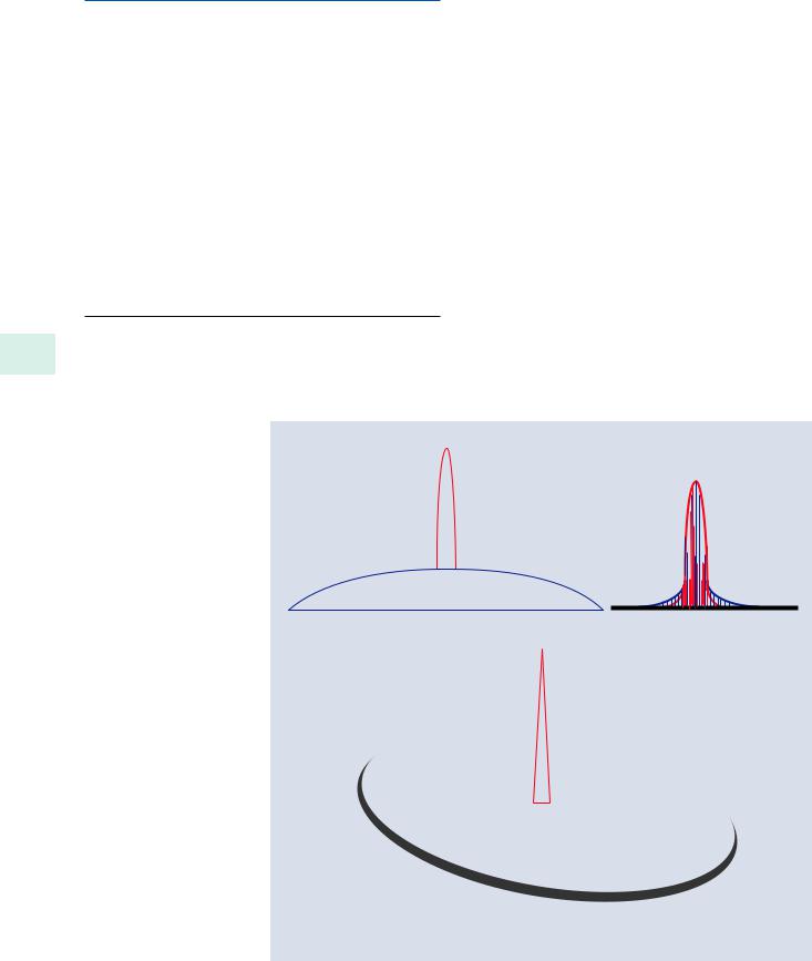
. Figure 10.11a shows schematically the narrow spatial dis- 10 tribution of the SE1 emitted from a finely focused beam superimposed on the broader spatial distribution of the of
. Fig. 10.11 a Schematic diagram of the SE1 and SE2 spatial
distributions for an intermediate a beam energy, e.g., E0 = 5–10 keV.
b Schematic diagram of the SE1 and SE2 spatial distributions for low beam energy, e.g., E0 = 1 keV. c Schematic diagram of the SE1 and SE2 spatial distributions
for high beam energy, e.g., E0 = 30 keV
c
the SE2 and SE3 that are created from the BSE distribution that would arise from a beam of intermediate energy, for example, 10 keV, on a material of intermediate atomic number, for example, Cu. While the beam can be focused to progressively smaller sizes within the limitations of the electron-optical system and the SE1 will follow the beam footprint as it is reduced, the BSE-SE2-SE3 distributions remain at a fixed size defined by the extent of the interaction volume, which depends primarily on the composition and the beam energy and is insensitive to small beam size. For the situation shown in . Fig. 10.11a, the SE1 distribution can interact over a short spatial range with a feature that has dimensions similar to the focused beam footprint, but the extended BSE-SE2-SE3 distribution interacts with this feature over a longer range. The BSE-SE2-SE3 create a long, gradually decreasing signal tail, so that a sharp feature appears blurred. There are two different strategies for improving the resolution by choosing the beam energy at the extreme limits of the SEM range.
Low Beam Energy Strategy
As the beam energy is lowered, the electron range decreases rapidly, varying approximately as E01.67. Since the BSE- SE2-SE3 distributions scale with the range, when the beam
SE1
b SE1+SE2
SE2
SE1
SE2
157 |
10 |
10.5 · Achieving High Resolution with Secondary Electrons
a
b
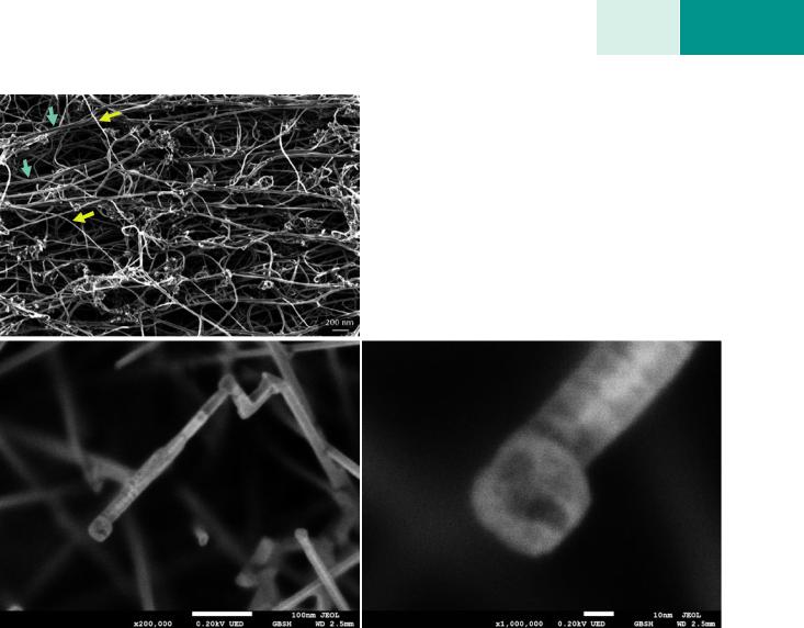
. Fig. 10.12 a High resolution achieved at low beam energy,
E0 = 1 keV: image of carbon nanofibers. Note broad fibers (cyan arrows) with bright edges and darker interiors and thin fibers (yellow arrows) for which the bright edge effects converge (Bar = 200 nm) (Example
courtesy John Notte, Zeiss). b High spatial resolution achieved at low landing energy: SnO2 whisker imaged with a landing energy of 0.2 keV (left, Bar = 100 nm) (right, Bar = 10 nm) (Images courtesy V. Robertson, JEOL)
energy is reduced so that E0 ≤2 keV, the situation illustrated in . Fig. 10.11b is reached for a finely focused beam (Joy 1984; Pawley 1984). The BSE-SE2-SE3 distributions collapse onto the SE1 distribution, and all the signals now represent high spatial resolution information. An example of carbon nanofibers imaged at E0 = 1 keV to achieve high resolution is shown in . Fig. 10.12a. In . Fig. 10.12a, the edges of the wider fibers appear bright (e.g., blue arrows) relative to the interior, as shown schematically in . Fig. 10.7a. . Figure 10.12 also illustrates the convergence of the bright edges of the narrow fibers (e.g., yellow arrows), as illustrated in
. Fig. 10.12b, to produce a very bright object against the background.
By applying a negative potential to the specimen, the landing energy can be reduced even further while preserving high spatial resolution, as shown in . Fig. 10.12b for tin oxide whiskers imaged with a TTL SE detector at a landing energy of E0 = 0.2 keV.
There are limitations of low beam energy operation that must be acknowledged (Pawley 1984). An inevitable consequence of low beam energy operation is the linear reduction in source brightness, which reduces the current that is contained in the focused probe which in turn affects feature visibility. Low energy beams are also more susceptible to interference from outside sources of electromagnetic radiation.
High Beam Energy Strategy
As the beam energy is increased, the electron range increases rapidly as E01.67, broadening the spatial distribution of the BSE-SE2-SE3 signals while the SE1 distribution remains fixed to the beam footprint. For example, when the beam energy is increased from 10 to 30 keV, the range increases by a factor of 6.3. With sufficient broadening, the spatial distributions of the BSE-SE2-SE3 signals do not significantly respond during beam scanning to small-scale features to which the SE1 are sensitive. The BSE-SE2-SE3 signals then represent
158\ Chapter 10 · High Resolution Imaging
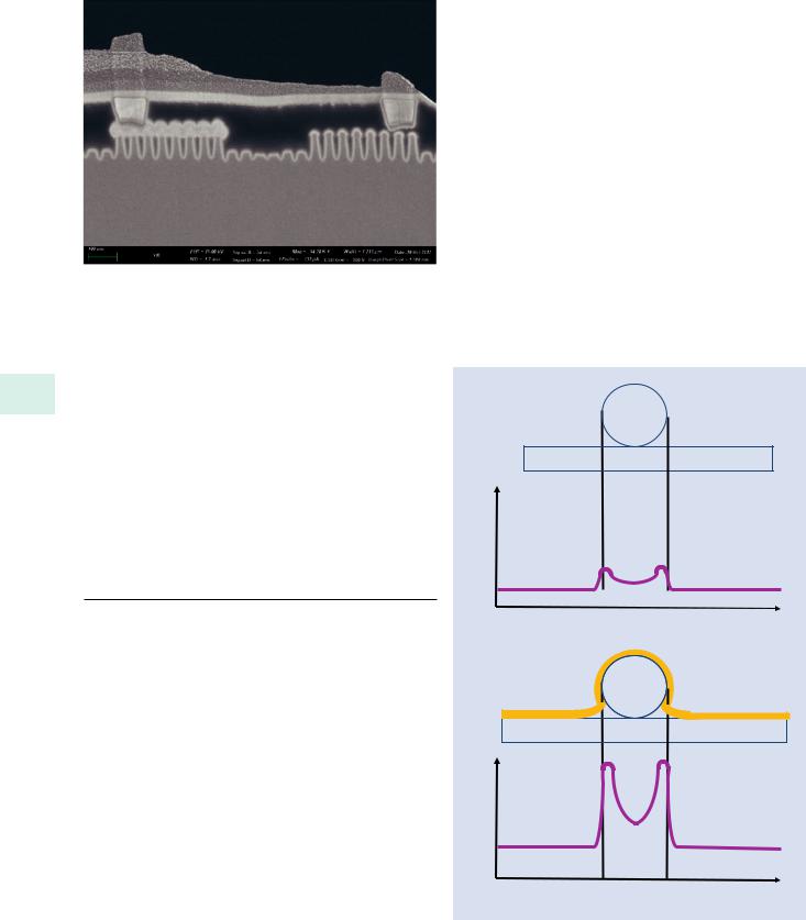
. Fig. 10.13 High resolution achieved at high beam energy, E0 = 15 keV: finFET transistor (16-nm technology) using the in lens SE detector in the Zeiss Auriga Cross beam. This cross section was prepared by inverted Ga FIB milling from backside (Bar = 100 nm) (Image courtesy of John Notte, Carl Zeiss)
10 a background noise component that, while it reduces the overall signal-to-noise, does not significantly alter the signal profiles across features. An advantage of operating at high beam energy is that the source brightness is increased, thus enabling more current to be obtained in a given focused probe size, which can help to compensate for the reduced signal-to-noise caused by the remote BSE-SE2-SE3 signals. An example of high beam energy imaging to achieve high resolution is shown in . Fig. 10.13.
10.5.2\ Improving theSE 1 Signal
Since the SE1 Signal Is So Critical To Achieving High Resolution, What Can Be Done To Improve It?
Excluding theSE 3 Component
For a bulk specimen, the high resolution SE1 component only forms 5–20% of the total SE signal collected by the E–T(positive bias) detector, while the lower resolution SE2 and SE3 components of roughly similar strength form the majority of the SE signal. While the SE1 and SE2 components are generated within 1 to 10 μm, the SE3 are produced millimeters to centimeters away from the specimen when the BSEs strike instrument components. This substantial physical separation is exploited by the class of “through-the-lens” (TTL) detectors, which utilize the strong magnetic field of the objective lens to capture the SE1 and SE2 which travel up the bore of the lens and are accelerated onto a scintillator-photomultiplier detector. Virtually all of the SE3 are excluded by their points of origin being outside of the lens magnetic field. For an SE1 component of 10% and SE2 and SE3 components of 45%, the ratio of high resolution/low resolution signals thus changes from 0.1 for the
E–T(positive bias) detector to 0.22 for the TTL detector.
Making More SE1: Apply a Thin High-δ Metal Coating
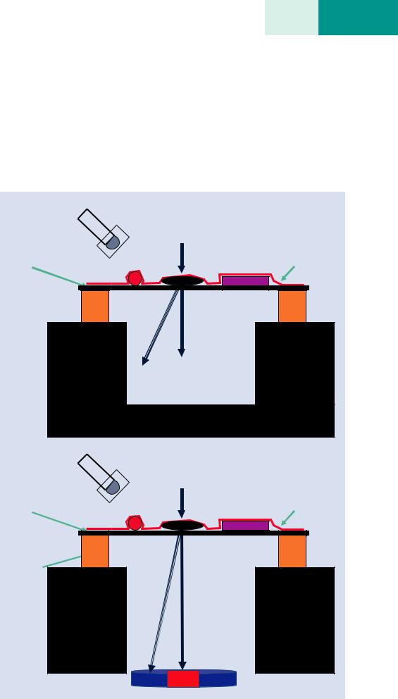
Because SEs are generated within a thin surface layer, the SE coefficient δ of the first few atomic layers will dominate the SE emission of the specimen. For specimens that consist of elements such as carbon with a low value of δ, the SE1 signal can be increased by applying a thin coating (one to a few nanometers) of a high SE emitter such as gold-palladium (rather than pure gold, which deposits as islands that can be mistaken for specimen structure), or platinum-family metals. While such a coating can also serve to dissipate charging from an insulating specimen, even for conducting carbonaceous materials the heavy-metal coating increases the surface SE1 emission of the specimen while not significantly increasing the scattering of beam electrons due to its minimal thickness so that BSE, SE2, and SE3 signals are not affected. As shown schematically in . Fig. 10.14a, the SE signal across an uncoated particle shows an increase at the edge due to the grazing beam incidence, but after a thin high-δ metal coating
a
SE signal
Scan position
b
SE signal
Scan position
. Fig. 10.14 Schematic illustration of the effect of heavy metal, high δ coating to increase contrast from low-Z targets: a SE signal trace from an uncoated particle; b signal trace after coating with thin Au-Pd
159 |
10 |
10.5 · Achieving High Resolution with Secondary Electrons
is applied (. Fig. 10.14b), the SE signal at the edges of features will be substantially enhanced.
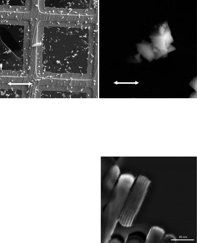
Making Fewer BSEs, SE2, and SE3 by Eliminating Bulk Scattering From the Substrate
For the important class of specimens such as nanoscale particles which have such small mass thickness that the beam electrons penetrate through the particle into the underlying bulk substrate, the large BSE, SE2 and SE3 components that
dominates the E–T(positive bias) signal respond to substrate properties and don’t actually represent specimen information at all. Thus, the high resolution imaging situation can be significantly improved by eliminating the bulk substrate. The particles are deposited on an ultrathin (~10-nm) carbon film supported on a metal (Cu, Ni, etc.) grid. This grid is placed over a deep blind hole drilled in a block of carbon that will serve as a Faraday cup for the beam electrons that pass though the particles, as shown schematically in . Fig. 10.15a. An example of this preparation is shown for particles of SRM470
. Fig. 10.15 a Schematic illustration of specimen mounting strategy to minimize background by eliminating the bulk substrate. b Scanning transmission electron microscopy (STEM) two component detector for high energy electrons: on-axis bright-field detector and surrounding annular dark-field detector
a
Everhart-Thornley detector
10 nm carbon foil
Grid bar, e.g., Cu
b
Everhart-Thornley detector
10 nm carbon foil
Grid bar, e.g., Cu
~10 nm carbon or high-d metal coating for discharging and stability
Deep blind hole in carbon
~10 nm carbon or high-d metal coating for discharging and stability
On-axis bright field detector
Annular dark-field detector
\160 Chapter 10 · High Resolution Imaging
K-309 particle shards on thin carbon
|
|
50 mm |
|
5 mm |
|
|
|
|
|
|
|
10 |
|
|
|
|
|
|
|
Conventional Everhart-Thornley (+bias) detector above specimen |
|||
|
|
||||
|
|
|
|
|
|
. Fig. 10.16 SEM imaging glass shards deposited on a thin (~ 10-nm carbon) at E0 = 20 keV and placed over a deep blind hole in a carbon block
(K411 glass) in . Fig. 10.16. By selecting operation at the highest beam energy available, for example, 20–30 keV, backscattering will be minimized along with the SE2 and SE3 signals.
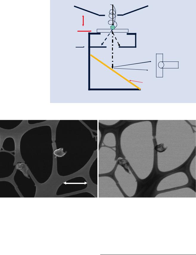
Scanning Transmission Electron Microscopy in the Scanning Electron Microscope (STEM-in-SEM)
The “thin film” support method for nanoscale particles and other thin specimens (either inherently thin or prepared as thin sections by ion beam milling) can be further exploited by collecting the beam electrons that transmit through the specimen to create a scanning transmission electron microscope (STEM) image, as illustrated in . Fig. 10.15b. To create the STEM image, an appropriate detector, such as a passive scintillator-photomultiplier, is placed below the specimen grid on the optical axis. The size of this detector is such that it accepts only electrons traveling close to the optical axis that pass through the specimen unscattered. Those electrons that experience even a small angle elastic scattering event that causes an angular deviation of a few degrees will miss the detector. Thus, the regions of the specimen with minimal scattering will appear bright, while those with sufficient mass to cause elastic scattering will appear dark, creating a “bright- field” image. A more elaborate STEM detector array can include an annular ring detector co-mounted with the central on-axis bright-field detector to capture the elastically scattered transmitted electrons from the specimen, as illustrated in . Fig. 10.15b. This off-axis annular detector produces a “dark-field” image since the thin regions such as the support film that do not produce significant scattering events
will appear dark. Portions of the specimen that do scatter sufficiently will appear bright. Since elastic scattering depends strongly on local atomic number, compositional effects can be observed in the dark field STEM image. An example of a high resolution STEM-in-SEM image created with an annular off-axis detector is shown in . Fig. 10.17.
. Fig. 10.17 Dark-field annular detector STEM image of BaFe12O19 nanoparticles; E0 = 22 keV using oriented dark-field detector in the Zeiss Gemini SEM. The 1.1-nm (002) lattice spacing is clearly evident (Image courtesy of John Notte, Carl Zeiss. Image processed with ImageJ-Fiji CLAHE function)
10.5 · Achieving High Resolution with Secondary Electrons
. Fig. 10.18 Schematic |
|
|
cross section of a STEM-in-SEM |
|
|
detector that makes use of the |
|
|
Everhart–Thornley(positive bias) |
Short |
|
detector to form a bright-field |
||
working |
||
STEM image |
||
distance, ~ 3 mm |
||
|
161 |
|
10 |
|
|
|
Through the lens detector: SE image
C-film and |
|
|
support grid |
Scattered |
|
|
||
|
beam |
|
Aperture |
electrons |
|
E-T detector: “STEM Image” |
||
|
||
Electrons |
Unscattered beam electrons |
|
scattered by |
||
|
||
particle are |
|
|
cut off by |
|
|
aperture |
|
|
|
Au surface |
Simple STEM-in-SEM detector
Aerosol particles collected on lacey carbon 25 keV cold-FEG-SEM
a |
b |
500 nm
SEM (TTL) |
STEM (ET) |
. Fig. 10.19 Aerosol contamination particles deposited on lacey-carbon film and simultaneously imaged with a TTL detector for SE1 and the STEM-in-SEM detector shown in . Fig. 10.18 (Example courtesy John Small, NIST)
A simple STEM-in-SEM bright-field detector can be created as shown in . Fig. 10.18. The grid carrying the thin specimen is placed over an aperture that serves to stop electrons that have suffered an elastic scattering event in the specimen. The unscattered beam electrons pass through this aperture and strike a gold-covered surface below, where they generate strong SE emission, which is then attracted to the E–T(positive bias) detector, creating a bright-field image. If the SEM is also equipped with a TTL detector, the nearly pure SE1 image that arises from a thin specimen can be collected with the TTL detector simultaneously with the bright-field
STEM image collected with the E–T(positive bias) detector, as shown for particles supported on a lacey-carbon film in
. Fig. 10.19.
10.5.3\ Eliminate the Use of SEs Altogether:
“Low Loss BSEs“
BSEs are usually considered a low resolution signal because of the substantial delocalization that results from multiple elastic scattering of the beam electrons at conventional beam
\162 Chapter 10 · High Resolution Imaging
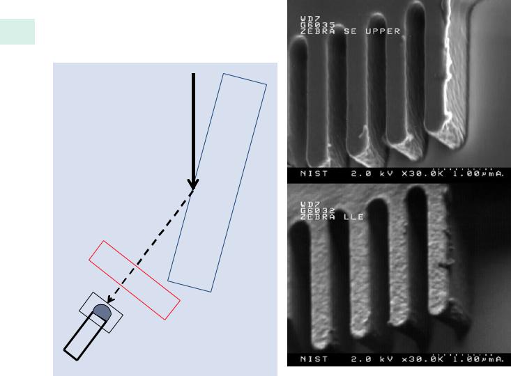
energy, for example, E0 ≥10 keV. However, high resolution SEM can be achieved by eliminating the use of SEs as the imaging signal and instead relying on the BSEs, specifically those that have lost very little of the initial beam energy. Because of the energy loss due to inelastic scattering that occurs for high energy beam electrons at a nearly constant rate, dE/ds, with distance traveled in the specimen, low loss BSEs represent beam electrons that have emerged from the specimen after traveling very short paths through the specimen. These low loss electrons are thus sensitive to specimen scattering properties very close to the entrance beam footprint and from a very shallow surface region, thus constituting a high resolution signal. Wells (1974a, b) first demonstrated the utility of this approach by using an energy filter to select the “low loss” backscattered electrons (LL BSE) that had lost less than a specified fraction, for example, 5 %, of the initial beam energy. At normal beam incidence, the LL BSE fraction of the total BSE population is very low, and their trajectories are spread over a wide angular range, the 2π azimuth around the beam, making their efficient collection difficult. The population of LL BSE can be increased, and their angular spread greatly decreased, by tilting the speci-
10 men to a high angle, for example, 70° or higher. As shown schematically in . Fig. 10.20, at this tilt angle a single elastic
E0
BSE
E0 - E
Energy filter -V + V
Post-acceleration detector, e.g. E-T detector
scattering event greater than 20°, which also has a suitable azimuthal angular component along the trajectory, can carry the beam electron out of the specimen as a low loss BSE after traveling along a short path within the specimen. The energy filter with an applied potential V + V then serves to decelerate and exclude BSEs that have lost more than a specified E of the incident energy. Since the electrons that pass through the filter have been retarded to a low kinetic energy, the detector following the filter must include an acceleration field, such as that of the Everhart–Thornley detector, to raise the kinetic energy to a detectable level for detection.
An example comparing TTL SE and LL BSE (10 % energy window) images of etched photoresist at low beam energy (E0 = 2 keV) is shown in . Fig. 10.21 (Postek et al. 2001). Note the enhanced surface detail visible on the top of the resist pattern in the LL BSE image compared to the SE image. The extreme directionality of the LL BSE detector leads to loss of signal on surfaces not tilted toward the detector, resulting in
. Fig. 10.20 Schematic illustration of low loss BSE imaging from a highly tilted specimen using an energy filter
. Fig. 10.21 SE (upper) and low loss BSE (lower) images of photoresist at E0 = 2 keV. Note the enhanced detail visible on the surface of the LL-BSE image compared to the SE image (Postek et al. 2001)