

- •Preface
- •Imaging Microscopic Features
- •Measuring the Crystal Structure
- •References
- •Contents
- •1.4 Simulating the Effects of Elastic Scattering: Monte Carlo Calculations
- •What Are the Main Features of the Beam Electron Interaction Volume?
- •How Does the Interaction Volume Change with Composition?
- •How Does the Interaction Volume Change with Incident Beam Energy?
- •How Does the Interaction Volume Change with Specimen Tilt?
- •1.5 A Range Equation To Estimate the Size of the Interaction Volume
- •References
- •2: Backscattered Electrons
- •2.1 Origin
- •2.2.1 BSE Response to Specimen Composition (η vs. Atomic Number, Z)
- •SEM Image Contrast with BSE: “Atomic Number Contrast”
- •SEM Image Contrast: “BSE Topographic Contrast—Number Effects”
- •2.2.3 Angular Distribution of Backscattering
- •Beam Incident at an Acute Angle to the Specimen Surface (Specimen Tilt > 0°)
- •SEM Image Contrast: “BSE Topographic Contrast—Trajectory Effects”
- •2.2.4 Spatial Distribution of Backscattering
- •Depth Distribution of Backscattering
- •Radial Distribution of Backscattered Electrons
- •2.3 Summary
- •References
- •3: Secondary Electrons
- •3.1 Origin
- •3.2 Energy Distribution
- •3.3 Escape Depth of Secondary Electrons
- •3.8 Spatial Characteristics of Secondary Electrons
- •References
- •4: X-Rays
- •4.1 Overview
- •4.2 Characteristic X-Rays
- •4.2.1 Origin
- •4.2.2 Fluorescence Yield
- •4.2.3 X-Ray Families
- •4.2.4 X-Ray Nomenclature
- •4.2.6 Characteristic X-Ray Intensity
- •Isolated Atoms
- •X-Ray Production in Thin Foils
- •X-Ray Intensity Emitted from Thick, Solid Specimens
- •4.3 X-Ray Continuum (bremsstrahlung)
- •4.3.1 X-Ray Continuum Intensity
- •4.3.3 Range of X-ray Production
- •4.4 X-Ray Absorption
- •4.5 X-Ray Fluorescence
- •References
- •5.1 Electron Beam Parameters
- •5.2 Electron Optical Parameters
- •5.2.1 Beam Energy
- •Landing Energy
- •5.2.2 Beam Diameter
- •5.2.3 Beam Current
- •5.2.4 Beam Current Density
- •5.2.5 Beam Convergence Angle, α
- •5.2.6 Beam Solid Angle
- •5.2.7 Electron Optical Brightness, β
- •Brightness Equation
- •5.2.8 Focus
- •Astigmatism
- •5.3 SEM Imaging Modes
- •5.3.1 High Depth-of-Field Mode
- •5.3.2 High-Current Mode
- •5.3.3 Resolution Mode
- •5.3.4 Low-Voltage Mode
- •5.4 Electron Detectors
- •5.4.1 Important Properties of BSE and SE for Detector Design and Operation
- •Abundance
- •Angular Distribution
- •Kinetic Energy Response
- •5.4.2 Detector Characteristics
- •Angular Measures for Electron Detectors
- •Elevation (Take-Off) Angle, ψ, and Azimuthal Angle, ζ
- •Solid Angle, Ω
- •Energy Response
- •Bandwidth
- •5.4.3 Common Types of Electron Detectors
- •Backscattered Electrons
- •Passive Detectors
- •Scintillation Detectors
- •Semiconductor BSE Detectors
- •5.4.4 Secondary Electron Detectors
- •Everhart–Thornley Detector
- •Through-the-Lens (TTL) Electron Detectors
- •TTL SE Detector
- •TTL BSE Detector
- •Measuring the DQE: BSE Semiconductor Detector
- •References
- •6: Image Formation
- •6.1 Image Construction by Scanning Action
- •6.2 Magnification
- •6.3 Making Dimensional Measurements With the SEM: How Big Is That Feature?
- •Using a Calibrated Structure in ImageJ-Fiji
- •6.4 Image Defects
- •6.4.1 Projection Distortion (Foreshortening)
- •6.4.2 Image Defocusing (Blurring)
- •6.5 Making Measurements on Surfaces With Arbitrary Topography: Stereomicroscopy
- •6.5.1 Qualitative Stereomicroscopy
- •Fixed beam, Specimen Position Altered
- •Fixed Specimen, Beam Incidence Angle Changed
- •6.5.2 Quantitative Stereomicroscopy
- •Measuring a Simple Vertical Displacement
- •References
- •7: SEM Image Interpretation
- •7.1 Information in SEM Images
- •7.2.2 Calculating Atomic Number Contrast
- •Establishing a Robust Light-Optical Analogy
- •Getting It Wrong: Breaking the Light-Optical Analogy of the Everhart–Thornley (Positive Bias) Detector
- •Deconstructing the SEM/E–T Image of Topography
- •SUM Mode (A + B)
- •DIFFERENCE Mode (A−B)
- •References
- •References
- •9: Image Defects
- •9.1 Charging
- •9.1.1 What Is Specimen Charging?
- •9.1.3 Techniques to Control Charging Artifacts (High Vacuum Instruments)
- •Observing Uncoated Specimens
- •Coating an Insulating Specimen for Charge Dissipation
- •Choosing the Coating for Imaging Morphology
- •9.2 Radiation Damage
- •9.3 Contamination
- •References
- •10: High Resolution Imaging
- •10.2 Instrumentation Considerations
- •10.4.1 SE Range Effects Produce Bright Edges (Isolated Edges)
- •10.4.4 Too Much of a Good Thing: The Bright Edge Effect Hinders Locating the True Position of an Edge for Critical Dimension Metrology
- •10.5.1 Beam Energy Strategies
- •Low Beam Energy Strategy
- •High Beam Energy Strategy
- •Making More SE1: Apply a Thin High-δ Metal Coating
- •Making Fewer BSEs, SE2, and SE3 by Eliminating Bulk Scattering From the Substrate
- •10.6 Factors That Hinder Achieving High Resolution
- •10.6.2 Pathological Specimen Behavior
- •Contamination
- •Instabilities
- •References
- •11: Low Beam Energy SEM
- •11.3 Selecting the Beam Energy to Control the Spatial Sampling of Imaging Signals
- •11.3.1 Low Beam Energy for High Lateral Resolution SEM
- •11.3.2 Low Beam Energy for High Depth Resolution SEM
- •11.3.3 Extremely Low Beam Energy Imaging
- •References
- •12.1.1 Stable Electron Source Operation
- •12.1.2 Maintaining Beam Integrity
- •12.1.4 Minimizing Contamination
- •12.3.1 Control of Specimen Charging
- •12.5 VPSEM Image Resolution
- •References
- •13: ImageJ and Fiji
- •13.1 The ImageJ Universe
- •13.2 Fiji
- •13.3 Plugins
- •13.4 Where to Learn More
- •References
- •14: SEM Imaging Checklist
- •14.1.1 Conducting or Semiconducting Specimens
- •14.1.2 Insulating Specimens
- •14.2 Electron Signals Available
- •14.2.1 Beam Electron Range
- •14.2.2 Backscattered Electrons
- •14.2.3 Secondary Electrons
- •14.3 Selecting the Electron Detector
- •14.3.2 Backscattered Electron Detectors
- •14.3.3 “Through-the-Lens” Detectors
- •14.4 Selecting the Beam Energy for SEM Imaging
- •14.4.4 High Resolution SEM Imaging
- •Strategy 1
- •Strategy 2
- •14.5 Selecting the Beam Current
- •14.5.1 High Resolution Imaging
- •14.5.2 Low Contrast Features Require High Beam Current and/or Long Frame Time to Establish Visibility
- •14.6 Image Presentation
- •14.6.1 “Live” Display Adjustments
- •14.6.2 Post-Collection Processing
- •14.7 Image Interpretation
- •14.7.1 Observer’s Point of View
- •14.7.3 Contrast Encoding
- •14.8.1 VPSEM Advantages
- •14.8.2 VPSEM Disadvantages
- •15: SEM Case Studies
- •15.1 Case Study: How High Is That Feature Relative to Another?
- •15.2 Revealing Shallow Surface Relief
- •16.1.2 Minor Artifacts: The Si-Escape Peak
- •16.1.3 Minor Artifacts: Coincidence Peaks
- •16.1.4 Minor Artifacts: Si Absorption Edge and Si Internal Fluorescence Peak
- •16.2 “Best Practices” for Electron-Excited EDS Operation
- •16.2.1 Operation of the EDS System
- •Choosing the EDS Time Constant (Resolution and Throughput)
- •Choosing the Solid Angle of the EDS
- •Selecting a Beam Current for an Acceptable Level of System Dead-Time
- •16.3.1 Detector Geometry
- •16.3.2 Process Time
- •16.3.3 Optimal Working Distance
- •16.3.4 Detector Orientation
- •16.3.5 Count Rate Linearity
- •16.3.6 Energy Calibration Linearity
- •16.3.7 Other Items
- •16.3.8 Setting Up a Quality Control Program
- •Using the QC Tools Within DTSA-II
- •Creating a QC Project
- •Linearity of Output Count Rate with Live-Time Dose
- •Resolution and Peak Position Stability with Count Rate
- •Solid Angle for Low X-ray Flux
- •Maximizing Throughput at Moderate Resolution
- •References
- •17: DTSA-II EDS Software
- •17.1 Getting Started With NIST DTSA-II
- •17.1.1 Motivation
- •17.1.2 Platform
- •17.1.3 Overview
- •17.1.4 Design
- •Simulation
- •Quantification
- •Experiment Design
- •Modeled Detectors (. Fig. 17.1)
- •Window Type (. Fig. 17.2)
- •The Optimal Working Distance (. Figs. 17.3 and 17.4)
- •Elevation Angle
- •Sample-to-Detector Distance
- •Detector Area
- •Crystal Thickness
- •Number of Channels, Energy Scale, and Zero Offset
- •Resolution at Mn Kα (Approximate)
- •Azimuthal Angle
- •Gold Layer, Aluminum Layer, Nickel Layer
- •Dead Layer
- •Zero Strobe Discriminator (. Figs. 17.7 and 17.8)
- •Material Editor Dialog (. Figs. 17.9, 17.10, 17.11, 17.12, 17.13, and 17.14)
- •17.2.1 Introduction
- •17.2.2 Monte Carlo Simulation
- •17.2.4 Optional Tables
- •References
- •18: Qualitative Elemental Analysis by Energy Dispersive X-Ray Spectrometry
- •18.1 Quality Assurance Issues for Qualitative Analysis: EDS Calibration
- •18.2 Principles of Qualitative EDS Analysis
- •Exciting Characteristic X-Rays
- •Fluorescence Yield
- •X-ray Absorption
- •Si Escape Peak
- •Coincidence Peaks
- •18.3 Performing Manual Qualitative Analysis
- •Beam Energy
- •Choosing the EDS Resolution (Detector Time Constant)
- •Obtaining Adequate Counts
- •18.4.1 Employ the Available Software Tools
- •18.4.3 Lower Photon Energy Region
- •18.4.5 Checking Your Work
- •18.5 A Worked Example of Manual Peak Identification
- •References
- •19.1 What Is a k-ratio?
- •19.3 Sets of k-ratios
- •19.5 The Analytical Total
- •19.6 Normalization
- •19.7.1 Oxygen by Assumed Stoichiometry
- •19.7.3 Element by Difference
- •19.8 Ways of Reporting Composition
- •19.8.1 Mass Fraction
- •19.8.2 Atomic Fraction
- •19.8.3 Stoichiometry
- •19.8.4 Oxide Fractions
- •Example Calculations
- •19.9 The Accuracy of Quantitative Electron-Excited X-ray Microanalysis
- •19.9.1 Standards-Based k-ratio Protocol
- •19.9.2 “Standardless Analysis”
- •19.10 Appendix
- •19.10.1 The Need for Matrix Corrections To Achieve Quantitative Analysis
- •19.10.2 The Physical Origin of Matrix Effects
- •19.10.3 ZAF Factors in Microanalysis
- •X-ray Generation With Depth, φ(ρz)
- •X-ray Absorption Effect, A
- •X-ray Fluorescence, F
- •References
- •20.2 Instrumentation Requirements
- •20.2.1 Choosing the EDS Parameters
- •EDS Spectrum Channel Energy Width and Spectrum Energy Span
- •EDS Time Constant (Resolution and Throughput)
- •EDS Calibration
- •EDS Solid Angle
- •20.2.2 Choosing the Beam Energy, E0
- •20.2.3 Measuring the Beam Current
- •20.2.4 Choosing the Beam Current
- •Optimizing Analysis Strategy
- •20.3.4 Ba-Ti Interference in BaTiSi3O9
- •20.4 The Need for an Iterative Qualitative and Quantitative Analysis Strategy
- •20.4.2 Analysis of a Stainless Steel
- •20.5 Is the Specimen Homogeneous?
- •20.6 Beam-Sensitive Specimens
- •20.6.1 Alkali Element Migration
- •20.6.2 Materials Subject to Mass Loss During Electron Bombardment—the Marshall-Hall Method
- •Thin Section Analysis
- •Bulk Biological and Organic Specimens
- •References
- •21: Trace Analysis by SEM/EDS
- •21.1 Limits of Detection for SEM/EDS Microanalysis
- •21.2.1 Estimating CDL from a Trace or Minor Constituent from Measuring a Known Standard
- •21.2.2 Estimating CDL After Determination of a Minor or Trace Constituent with Severe Peak Interference from a Major Constituent
- •21.3 Measurements of Trace Constituents by Electron-Excited Energy Dispersive X-ray Spectrometry
- •The Inevitable Physics of Remote Excitation Within the Specimen: Secondary Fluorescence Beyond the Electron Interaction Volume
- •Simulation of Long-Range Secondary X-ray Fluorescence
- •NIST DTSA II Simulation: Vertical Interface Between Two Regions of Different Composition in a Flat Bulk Target
- •NIST DTSA II Simulation: Cubic Particle Embedded in a Bulk Matrix
- •21.5 Summary
- •References
- •22.1.2 Low Beam Energy Analysis Range
- •22.2 Advantage of Low Beam Energy X-Ray Microanalysis
- •22.2.1 Improved Spatial Resolution
- •22.3 Challenges and Limitations of Low Beam Energy X-Ray Microanalysis
- •22.3.1 Reduced Access to Elements
- •22.3.3 At Low Beam Energy, Almost Everything Is Found To Be Layered
- •Analysis of Surface Contamination
- •References
- •23: Analysis of Specimens with Special Geometry: Irregular Bulk Objects and Particles
- •23.2.1 No Chemical Etching
- •23.3 Consequences of Attempting Analysis of Bulk Materials With Rough Surfaces
- •23.4.1 The Raw Analytical Total
- •23.4.2 The Shape of the EDS Spectrum
- •23.5 Best Practices for Analysis of Rough Bulk Samples
- •23.6 Particle Analysis
- •Particle Sample Preparation: Bulk Substrate
- •The Importance of Beam Placement
- •Overscanning
- •“Particle Mass Effect”
- •“Particle Absorption Effect”
- •The Analytical Total Reveals the Impact of Particle Effects
- •Does Overscanning Help?
- •23.6.6 Peak-to-Background (P/B) Method
- •Specimen Geometry Severely Affects the k-ratio, but Not the P/B
- •Using the P/B Correspondence
- •23.7 Summary
- •References
- •24: Compositional Mapping
- •24.2 X-Ray Spectrum Imaging
- •24.2.1 Utilizing XSI Datacubes
- •24.2.2 Derived Spectra
- •SUM Spectrum
- •MAXIMUM PIXEL Spectrum
- •24.3 Quantitative Compositional Mapping
- •24.4 Strategy for XSI Elemental Mapping Data Collection
- •24.4.1 Choosing the EDS Dead-Time
- •24.4.2 Choosing the Pixel Density
- •24.4.3 Choosing the Pixel Dwell Time
- •“Flash Mapping”
- •High Count Mapping
- •References
- •25.1 Gas Scattering Effects in the VPSEM
- •25.1.1 Why Doesn’t the EDS Collimator Exclude the Remote Skirt X-Rays?
- •25.2 What Can Be Done To Minimize gas Scattering in VPSEM?
- •25.2.2 Favorable Sample Characteristics
- •Particle Analysis
- •25.2.3 Unfavorable Sample Characteristics
- •References
- •26.1 Instrumentation
- •26.1.2 EDS Detector
- •26.1.3 Probe Current Measurement Device
- •Direct Measurement: Using a Faraday Cup and Picoammeter
- •A Faraday Cup
- •Electrically Isolated Stage
- •Indirect Measurement: Using a Calibration Spectrum
- •26.1.4 Conductive Coating
- •26.2 Sample Preparation
- •26.2.1 Standard Materials
- •26.2.2 Peak Reference Materials
- •26.3 Initial Set-Up
- •26.3.1 Calibrating the EDS Detector
- •Selecting a Pulse Process Time Constant
- •Energy Calibration
- •Quality Control
- •Sample Orientation
- •Detector Position
- •Probe Current
- •26.4 Collecting Data
- •26.4.1 Exploratory Spectrum
- •26.4.2 Experiment Optimization
- •26.4.3 Selecting Standards
- •26.4.4 Reference Spectra
- •26.4.5 Collecting Standards
- •26.4.6 Collecting Peak-Fitting References
- •26.5 Data Analysis
- •26.5.2 Quantification
- •26.6 Quality Check
- •Reference
- •27.2 Case Study: Aluminum Wire Failures in Residential Wiring
- •References
- •28: Cathodoluminescence
- •28.1 Origin
- •28.2 Measuring Cathodoluminescence
- •28.3 Applications of CL
- •28.3.1 Geology
- •Carbonado Diamond
- •Ancient Impact Zircons
- •28.3.2 Materials Science
- •Semiconductors
- •Lead-Acid Battery Plate Reactions
- •28.3.3 Organic Compounds
- •References
- •29.1.1 Single Crystals
- •29.1.2 Polycrystalline Materials
- •29.1.3 Conditions for Detecting Electron Channeling Contrast
- •Specimen Preparation
- •Instrument Conditions
- •29.2.1 Origin of EBSD Patterns
- •29.2.2 Cameras for EBSD Pattern Detection
- •29.2.3 EBSD Spatial Resolution
- •29.2.5 Steps in Typical EBSD Measurements
- •Sample Preparation for EBSD
- •Align Sample in the SEM
- •Check for EBSD Patterns
- •Adjust SEM and Select EBSD Map Parameters
- •Run the Automated Map
- •29.2.6 Display of the Acquired Data
- •29.2.7 Other Map Components
- •29.2.10 Application Example
- •Application of EBSD To Understand Meteorite Formation
- •29.2.11 Summary
- •Specimen Considerations
- •EBSD Detector
- •Selection of Candidate Crystallographic Phases
- •Microscope Operating Conditions and Pattern Optimization
- •Selection of EBSD Acquisition Parameters
- •Collect the Orientation Map
- •References
- •30.1 Introduction
- •30.2 Ion–Solid Interactions
- •30.3 Focused Ion Beam Systems
- •30.5 Preparation of Samples for SEM
- •30.5.1 Cross-Section Preparation
- •30.5.2 FIB Sample Preparation for 3D Techniques and Imaging
- •30.6 Summary
- •References
- •31: Ion Beam Microscopy
- •31.1 What Is So Useful About Ions?
- •31.2 Generating Ion Beams
- •31.3 Signal Generation in the HIM
- •31.5 Patterning with Ion Beams
- •31.7 Chemical Microanalysis with Ion Beams
- •References
- •Appendix
- •A Database of Electron–Solid Interactions
- •A Database of Electron–Solid Interactions
- •Introduction
- •Backscattered Electrons
- •Secondary Yields
- •Stopping Powers
- •X-ray Ionization Cross Sections
- •Conclusions
- •References
- •Index
- •Reference List
- •Index
\496 Chapter 29 · Characterizing Crystalline Materials in the SEM
29
50 µm
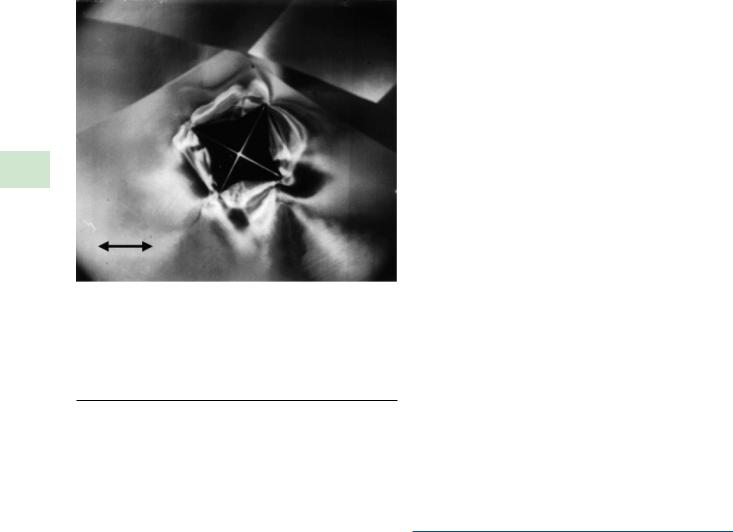
. Fig. 29.8 Electron channeling contrast from grains in polycrystalline Ni deformed by a diamond indentation placed in a single grain; E0 = 20 keV; BSE detector
29.1.3\ Conditions for Detecting Electron Channeling Contrast
Specimen Preparation
Channeling contrast effects are created in a shallow near- surface layer that is 10–100 nm in depth, depending on the incident beam energy and the material, where the incident beam has not yet undergone sufficient elastic scatter to destroy the initial beam collimation. Thus, the condition of the sample surface is of extreme importance for a successful channeling contrast measurement. The low level of channeling contrast, 2–5 %, also requires eliminating other competing sources of contrast, especially surface topography. Thus, a typical sample preparation will involve grinding and polishing to achieve a flat, topography-free surface. However, the inevitable surface damage layer produced in many materials, especially metals, by mechanical abrasion, including the “Beilby layer” that remains after the final polishing with the finest scale abrasives, must be removed by chemical or electrochemical polishing or low energy ion beam sputtering. (Note that high energy ion sputtering can produce sub- surface damage that can destroy electron channeling contrast.)
Instrument Conditions
Detecting channeling effects that produce weak contrast in the range 2–5 % in an SEM image requires careful choice of operating conditions. The low contrast creates a requirement for a high threshold current, so that typically a beam current of 10 nA or more is needed when scanning at rapid frame rates to find features of interest. After such features have been located, a smaller beam diameter can be used to improve resolution at the inevitable cost of a lower beam current, which then requires a longer frame time to maintain contrast
visibility. Because a small convergence angle is also desirable to maximize channeling contrast, a high electron source brightness is important to maximize the beam current into a focused beam of useful size. A high beam energy in the range from 10 to 30 keV is desirable both to increase source brightness and to create high energy BSEs for efficient detection. Channeling contrast is carried by the high energy fraction of the backscattered electrons, and to maximize that signal, a large solid angle BSE detector (solid state or passive scintillator) is the best choice with the specimen set normal to the beam. The positively biased Everhart–Thornley (E–T) detector, with its high efficiency for BSEs through capture of the SE2 and SE3 signals, is also satisfactory. Because of the weak contrast, the live image display must be enhanced by careful adjustment of the “black level” and amplifier settings to spread the channeling contrast over the full black-to-white range of the final display to render channeling contrast visible. Post-collection image processing by various tools, e.g., CLAHE in ImageJ-Fiji, can be very effective at recovering fine scale details.
Crystallographic contrast by electron channeling provides images of the crystallographic microstructure of materials. For many applications in materials science, it is also important to measure the actual orientation of the microstructure on a local basis with high spatial resolution of 1 micrometer laterally or even finer. The technique of electron backscatter diffraction (EBSD) patterns provides the ideal complement to channeling contrast microscopy.
29.2\ Electron Backscatter Diffraction
in the Scanning Electron Microscope
An understanding of the crystallography of a material is required to fully describe the structure property relationships that control a material’s physical properties. By linking the microstructure to the crystallography of the sample, a full picture of the sample can be developed. The development of electron backscattering diffraction (EBSD) equipment and its placement in commercial tools for phase identification and orientation determination has provided new insights into microstructure, crystallography and materials physical properties.
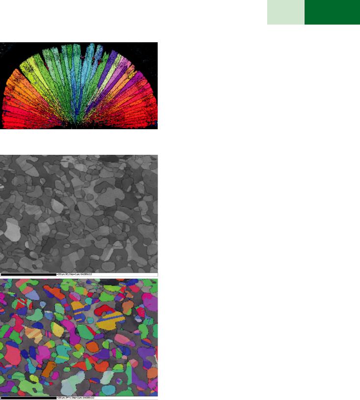
EBSD in the SEM has been developed for two different purposes. The oldest application of EBSD is for the measurement of texture on a grain by grain basis. Texture determined in this way is called the microtexture of the sample (Randle 2013). An example of this is . Fig. 29.9, where the point-by-point orientation of an assembly of ZnO crystals is shown where the color coding indicates the orientation of the crystal. The other use of EBSD is for the identification or discrimination of micrometer or sub-micrometer crystalline phases (Michael 2000; Dingley and Wright 2009).
. Figure 29.10 is an example of this, showing a dual-phase steel with both ferrite (body-centered cubic) and austenite
(face-centered cubic) present. EBSD can easily discriminate
497 |
29 |
29.2 · Electron Backscatter Diffraction in the Scanning Electron Microscope
. Fig. 29.9 Inverse pole figure map of ZnO crystals
a
b
. Fig. 29.10 EBSD of a dual phase steel that contains both austenite and ferrite. EBSD of multiphase samples can discriminate phases with different crystal structures. a This is a band contrast map, basically a measure of the pattern sharpness, which accurately reflects the grain structure of the sample. b Orientation map of the austenite phase while the ferrite is shown in the underlying band contrast image (Bar = 200 µm)
between these two crystal structures. Both applications add an important new tool to the SEM. The SEM now has the capability to study the morphology of a sample through either secondary or backscattered electron imaging, the
chemistry through energy dispersive spectrometry and the crystallography of the sample by electron channeling contrast imaging and EBSD. EBSD techniques have recently been developed that allow both the elastic and plastic strains present in a microstructure to be determined and this has been called high resolution EBSD or HREBSD. A more useful description would be high angular resolution EBSD. This technique is beyond the scope of this chapter (Wilkinson et al. 2006).
Microtexture is a term that means a population of individual orientations that are usually related to some feature of the sample microstructure. A simple example of this is the relationship of the individual grain size to grain orientation. The concept of microtexture may also be extended to include the misorientation between grains, often termed the mesotexture. It is now possible using EBSD to collect and analyze thousands of orientations per minute, thus allowing excellent statistics in various distributions. The ability to link texture and microstructure has enabled significant progress in the understanding of recrystallization, grain boundary structure and properties, grain growth and many other important physical phenomena.
The identification of phases in the SEM has usually been obtained by determining the composition of the phase and then inferring the identity of the phase. This technique is subject to the inherent inaccuracies in quantitative analysis in the SEM using EDS or WDS. In addition, this technique is not useful when one is attempting to identify a phase that has multiple crystal structures, but only one composition. A good example of this concern is TiO2, with three different crystal structures. Another important technological problem is the identification of austenite in ferrite in engineering steels. Austenite has a face centered cubic crystal structure and ferrite is body centered cubic and both phases may have very similar chemistries.
Improved resolution for EBSD has been achieved by utilizing thin samples that allow the transmission and diffraction of electrons using accelerating voltages (20–30 kV) achievable in the SEM. The patterns generated in this way have very similar characteristics to EBSD but are formed in transmission mode and thus, due to the thin sample, have much improved spatial resolution as compared to EBSD performed on bulk samples. Transmission Kikuchi diffraction (TKD) allows the microtexture of ultrafine grained crystalline materials to be studied (Keller and Geiss 2012; Trimby 2012).
In order to best use EBSD, it is helpful if the reader has some knowledge of crystallography and how crystallography is represented. There are a number of excellent books on this subject (McKie and McKie 1986; Rousseau 1998). This module will first describe the origin of the EBSD pattern in the SEM. The detectors or cameras used to detect EBSD patterns will be described. As sample preparation is critical to the success of an EBSD investigation, it is important to understand the methods needed to produce samples of appropriate quality. Finally, details of the actual experiment and the resulting output will be discussed.
\498 Chapter 29 · Characterizing Crystalline Materials in the SEM
29.2.1\ Origin of EBSD Patterns
EBSD patterns are obtained in the SEM by illuminating a highly tilted specimen with a stationary electron beam. The beam electrons interact with the sample and are initially inelastically scattered. There are two current methods that are employed. The first method (conventional EBSD) uses the sample in a mode where backscattered electrons are detected (i.e., from a bulk sample). The second method (often termed TKD or transmission-EBSD although the use
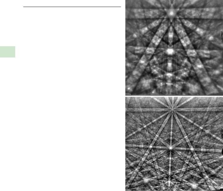
29 of the latter implies the impossibility of simultaneous transmission and backscattering of the electrons) relies on a very thin sample and the patterns are then formed by the transmitted electrons. In the case of the bulk sample and backscattered electron detection, the sample is held at a steep angle with respect to the electron beam. When a thin sample is used for TKD, the sample does not need to be tilted at such a high angle, and in fact the electron beam may be used to illuminate a sample which is not tilted. In either case, backscatter or transmission, some of these inelastically scattered electrons that have lost little of their original energy satisfy the diffraction condition with the crystalline planes within the sample. When this interaction happens near the surface of the sample these electrons escape and form the EBSD pattern that is observed. These backscattered electrons appear to originate from a virtual point below the surface of the specimen. These types of patterns were first described by Kikuchi and are often referred to as Kikuchi patterns (Randle 2013). Some of the backscattered electrons satisfy the Bragg conditions for diffraction (+θ and −θ) and are diffracted into cones of intensity with a semi-angle of (90-θ), with the cone axis normal to the diffracting plane. As shown by the Bragg Eq. (29.1), and . Table 29.1, the short wavelength of the electron (at typical accelerating voltages of 10–30 kV used in the SEM) results in a small Bragg angle of less than 2°. Each plane yields two cones of intensity. The cones are quite flat and when they intercept the imaging plane they are imaged as two nearly straight lines separated by an angle of twice the Bragg angle. An alternative but equivalent description is the single event model. In this model, it is argued that the inelastic and elastic scattering events are intimately related and may be thought of as one event. In this case the electron channels out of the sample and forms the EBSD pattern (Winkelmann 2009; Randle 2013). . Figure 29.11 are two examples of an EBSD patterns collected from the mineral hematite at 5 kV and 40 kV. Note that the Kikuchi bands appear as nearly straight lines. The effect of the accelerating voltage is clearly seen. As the accelerating voltage is increased the Bragg angle decreases resulting in more narrowly spaced Kikuchi bands in the patterns. It is also important to note that the patterns are fixed with respect to the crystal orientation and so the positions of the line traces in the patterns have not moved. Fortunately we need not understand the exact physics of EBSD pattern formation in order to use these patterns for crystallographic analysis.
a
b
. Fig. 29.11 EBSD patterns acquired from the mineral hematite (trigonal) that demonstrate the pattern changes that result from the acceleration voltage change. Note that as expected from the Bragg equation the band widths decrease with increasing accelerating voltage. a 5 kV, b 40 kV
EBSD patterns consist of what appear to be nearly straight bands (they are actually conic sections) which may have bright or dark centers with respect to the rest of the pattern. These straight bands are the Kikuchi lines discussed previously. The Kikuchi bands intersect in many locations and these are called zone axes which are actual crystallographic directions within the unit cell of the crystal. The angles between the Kikuchi bands and the angles between the zone axes are specific for a given crystal structure. These features can be seen in . Fig. 29.11b where the Kikuchi bands and the

499 |
29 |
29.2 · Electron Backscatter Diffraction in the Scanning Electron Microscope
zone axes are clearly visible. In high quality patterns as shown in . Fig. 29.11, there are many other features that are visible and may be used to understand the unit cell from which the pattern was collected.
29.2.2\ Cameras for EBSD Pattern Detection
It is relatively easy to collect EBSD patterns in the SEM. The earliest EBSD images were collected by directly exposing photographic emulsions inside the specimen chamber of the SEM. As discussed previously, EBSD patterns are obtained from bulk samples by illuminating a highly tilted surface with the electron beam and then collecting the patterns on a position sensitive detector, sometimes referred to as a camera, that is 1–2 cm from the tilted sample surface. Generally the detector surface is located normal to the sample tilt axis so that tilting of the sample is easily achieved but the detector may also be tilted a few tens of degrees away from the horizontal position. The first electronic capture of EBSD patterns utilized low-light video rate cameras that produced useable but somewhat noisy images requiring the use of very high beam currents in the SEM. Current EBSD cameras consist of a fluorescent screen, either circular or rectangular, that is about 2 cm in diameter if circular or 2 cm on a side if square or rectangular formats are utilized. The screen is coated with a thin Al coating to avoid charging and to exclude light. The fluorescent screen is kept thin so that it can be imaged from the opposite side using either a fiber optic bundle or a lens to transfer the image on the phosphor to a charge coupled device (CCD) or a CMOS type solid state imager. Camera designs strive to minimize the loss of light from the fluorescent screen to increase the speed at which patterns can be collected or to increase the quality of the detected patterns. The transfer optics must also be designed to minimize any optical distortions to the collected patterns (Schwarzer et al. 2009).
The imager should have a sufficient number of pixel elements so that the angular resolution is adequate for detection.
In addition, it is extremely useful to be able to bin the pixels in the detector. Binning pixels simply means that adjacent pixels are summed together (normally in specific patterns like 2 × 2 or 4 × 4) to increase the signal but with a decrease in pattern resolution. Currently, detectors are capable of collecting more than 1000 patterns per second when heavily binned and with sufficient electron beam current.
The entire detector must be mounted on a precision retractable stage. The precision retractable stage allows the detector assembly to be moved into the same position each time the detector is inserted to maintain the geometrical calibration of the system. It is important to position the detector close to the sample, generally the sample to detector distance should be on the order of or even slightly less than the fluorescent screen diameter so that a large portion of the EBSD pattern may be collected. The insertion mechanism is motorized to allow the camera to be moved into position in a matter of few seconds. A typical arrangement of the sample and
Detector
Sample
. Fig. 29.12 An image from the inside of an SEM sample region with the sample tilted for EBSD and the EBSD camera or detector inserted. Also note at the bottom of the detector screen there are small rectangular solid state electron detectors for imaging the sample while it is highly tilted. These detectors result in remarkable crystallographic contrast
the EBSD camera or detector is shown in . Fig. 29.12. Also visible at the bottom of the EBSD detector are the forescattered electron detectors. These solid state detectors provide excellent crystallographic contrast when the sample is highly tilted and standard backscattered or secondary electron imaging are not optimal.
29.2.3\ EBSD Spatial Resolution
It is important to understand the volume from which the diffraction pattern is generated in the SEM. In many applications the highest resolution is not required to utilize EBSD for the mapping of the texture of a microstructure. However, there are applications where high spatial resolution is required. Examples are the mapping of deformed microstructures or the study of fine grained materials.
The formation of EBSD patterns depends on the scattering and subsequent diffraction of electrons. Bragg’s Law describes the diffraction of specific wavelengths of electrons from the planes in a crystalline solid. If there is a large spread in the energy of the electrons that are exiting the sample surface we would not expect to see the lines that we see in our EBSD patterns due to diffraction. These lines are in nearly the exactly correct position as described by the Bragg diffraction of the electrons based on the beam voltage used to produce the patterns. From this we must conclude that the electrons leaving the surface are of nearly the same energy. Electrons that have lost larger amounts of energy contribute to the background intensity and do not contribute to the diffraction features that we want to observe (Deal et al. 2008).
500\ Chapter 29 · Characterizing Crystalline Materials in the SEM
a |
b |
29
c
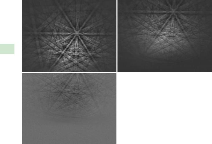
. Fig. 29.13 These series of EBSD patterns show the effect of sample tilt on the EBSD pattern quality. a 60°, b 50°, and c 40°
For EBSD, we tilt the sample at a high angle with respect to the electron beam. This tilt is important to obtaining the high quality patterns that are needed for EBSD. As shown in
. Fig. 29.13, the tilt angle has a large effect on the pattern quality. The best pattern qualities are obtained at higher tilt angles with some optimal condition between the pattern quality and the ease of imaging of the highly tilted sample.
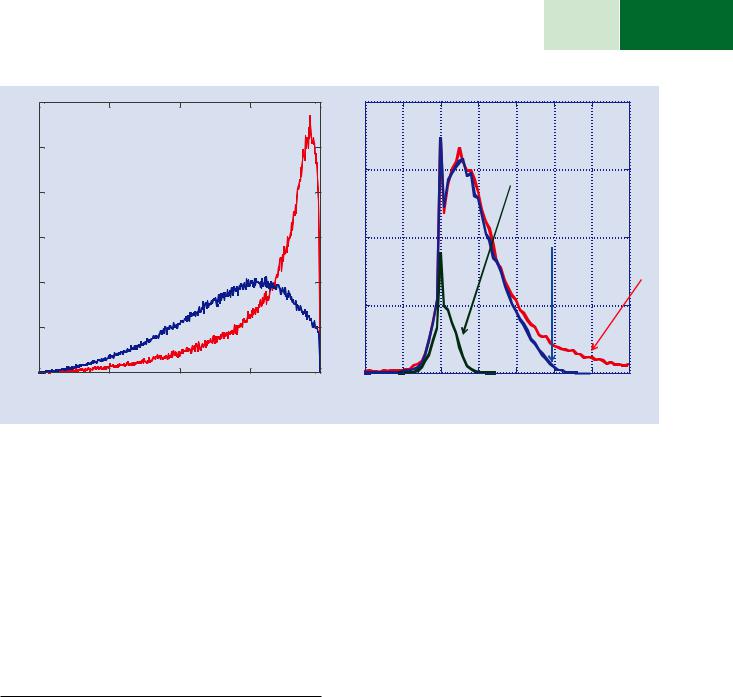
. Figure 29.14a shows the backscattered electron energy distribution that is developed from a highly titled sample (70° tilt) compared to 0° tilt. Note that the energy is highly peaked toward the operating voltage of the microscope at 70° tilt when compared to the same distribution from an electron beam that is normal to the sample surface. Further, since the EBSD pattern is clearly visible, they must form from only the electrons that have lost either no or a small amount of their energy. The electrons that have lost only a small amount of their energy are emitted from the sample in regions that are very close to the original beam foot print on the surface of the sample. This is shown in . Fig. 29.14b, which is a Monte Carlo simulation of the distance from the initial beam impact point that the electrons emerge from the sample surface for all the backscattered electrons, those that lost up to 2 kV and
those that lost only 0.2 kV. The pattern is formed from these low loss electrons and thus the resolution is quite good. Thus, although EBSD involves backscattered electrons, it is a technique with much higher spatial resolution than standard backscattered electron imaging. Typically, resolutions of better than 0.1 μm can be achieved for a beam voltage of 20 kV in the transition metals. The electrons that have lost larger amounts of energy will contribute the background intensity in the EBSD pattern. These electrons are the main reason why there is limited contrast in EBSD patterns without some form of background removal either through division or subtraction or some other computational method of removal (Michael and Goehner 1996).
The high tilt angle limits the spatial resolution attainable due to the elongation of the electron beam foot print on the sample surface. The resolution parallel to the tilt axis is much better than the resolution perpendicular to the tilt axis due to the high sample tilt angles used to acquire EBSD patterns. The resolution perpendicular to the tilt axis is related to the resolution parallel to the tilt axis by
Lperp = Lpara (1 / cos θ ) \ |
(29.3) |
29.2 · Electron Backscatter Diffraction in the Scanning Electron Microscope |
|
|
|
|
|
|
501 |
29 |
||||
|
|
|
|
|
|
|
|
|||||
a |
|
|
|
b |
|
|
|
|
|
|
|
|
electrons |
|
|
|
electrons |
|
|
|
|
>19.8 kV |
|
|
|
|
|
|
|
|
|
|
|
|
|
|
||
Backscattered# |
|
|
|
Backscattered# |
|
|
|
|
|
>18 kV |
|
|
|
|
|
|
|
|
|
|
|
|
|
|
|
|
|
|
|
|
|
|
|
|
|
|
All electrons |
|
0 |
5 |
10 |
15 |
20 |
200 |
100 |
0 |
–100 |
–200 |
–300 |
–400 |
–500 |
|
|
Energy (keV) |
|
|
|
|
|
Distance (nm) |
|
|
|
|
. Fig. 29.14 a Monte Carlo electron trajectory simulations of the backscattered electron distributions for Ni at 20 kV at a tilt of 70° (red) and for a sample at 0° tilt (blue) that is normal to the electron beam. b Backscattered
electron distributions from Ni at 20 kV and a sample tilt of 70° for different levels of energy loss as a function of distance from the beam impact point
where θ is the sample tilt with respect to the horizontal, Lperp is the resolution perpendicular to the tilt axis, and Lpara is the resolution parallel to the tilt axis. The resolution perpendicu-
lar to the tilt axis is roughly three times the resolution parallel to the tilt axis for a tilt angle of 70° and increases to 5.75 times for a tilt angle of 80°. Thus, it is best to work at the lowest sample tilt angles possible consistent with obtaining good EBSD patterns.
29.2.4\ How Does a Modern EBSD System
Index Patterns
Modern EBSD systems all use the same basic steps to go from a collected EBSD pattern to indexing and to the determination of the crystal orientation with respect to a reference frame. Once the pattern is collected, the necessary information for indexing of the pattern (indexing refers to assigning a consistent set of crystallographic directions to the pattern with respect to a given or a set of given candidate structures) must be derived from the diffraction pattern. Once the pattern has been indexed correctly (various vendors use different measures of what constitutes correct indexing), it is a simple matter to determine the crystallographic orientation represented by the EBSD pattern.
The most important factor in obtaining a quality orientation is that the system have good quality patterns for indexing. The quality of the detected patterns needed for a given experimental measurement can be influenced by choices made over how the camera is operated. EBSD patterns are of low inherent contrast mainly due to electrons that have lost
significant amounts of energy contributing to the overall intensity of the pattern background. To compensate for this, methods of removing the background are utilized. Some systems use a software-generated background to compensate for the background and increase the pattern contrast. A more established approach uses a background image obtained by scanning over a large number of grains that produce the background signal. This background is then used to normalize the raw EBSD pattern to produce a pattern with high contrast (Michael and Goehner 1996).
EBSD cameras are generally able to collect patterns at higher angular resolution per pixel than is needed for most orientation mapping. However, if high accuracy is needed, it is possible to use the full resolution of the camera to produce EBSD patterns. The disadvantage of using the full resolution of the EBSD camera is that longer exposure times are needed to produce usable EBSD patterns. This longer exposure can really slow down map acquisition. It is possible to bin the camera resolution, usually by factors of 2, to produce lower resolution patterns but with the ability to collect the patterns at a much higher collection rate. Thus, if the high angular resolution is not required, the camera should be used at a reduced resolution, (2 × 2, 4 × 4, or 8 × 8 binning) to speed up the acquisition. The tradeoff is between orientation accuracy and speed of the measurement.
Once the camera is set correctly for the given experiment, the patterns should be of high quality with good contrast. The next step is for the software to extract the line positions from the collected pattern. In all modern systems this is accomplished with an algorithm called the Hough Transform, which takes straight lines and transfers them into points